element14 Community
element14 Community
    Register Log In
  • Site
  • Search
  • Log In Register
  • About Us
  • Community Hub
    Community Hub
    • What's New on element14
    • Feedback and Support
    • Benefits of Membership
    • Personal Blogs
    • Members Area
    • Achievement Levels
  • Learn
    Learn
    • Ask an Expert
    • eBooks
    • element14 presents
    • Learning Center
    • Tech Spotlight
    • STEM Academy
    • Webinars, Training and Events
    • Learning Groups
  • Technologies
    Technologies
    • 3D Printing
    • FPGA
    • Industrial Automation
    • Internet of Things
    • Power & Energy
    • Sensors
    • Technology Groups
  • Challenges & Projects
    Challenges & Projects
    • Design Challenges
    • element14 presents Projects
    • Project14
    • Arduino Projects
    • Raspberry Pi Projects
    • Project Groups
  • Products
    Products
    • Arduino
    • Avnet Boards Community
    • Dev Tools
    • Manufacturers
    • Multicomp Pro
    • Product Groups
    • Raspberry Pi
    • RoadTests & Reviews
  • Store
    Store
    • Visit Your Store
    • Choose another store...
      • Europe
      •  Austria (German)
      •  Belgium (Dutch, French)
      •  Bulgaria (Bulgarian)
      •  Czech Republic (Czech)
      •  Denmark (Danish)
      •  Estonia (Estonian)
      •  Finland (Finnish)
      •  France (French)
      •  Germany (German)
      •  Hungary (Hungarian)
      •  Ireland
      •  Israel
      •  Italy (Italian)
      •  Latvia (Latvian)
      •  
      •  Lithuania (Lithuanian)
      •  Netherlands (Dutch)
      •  Norway (Norwegian)
      •  Poland (Polish)
      •  Portugal (Portuguese)
      •  Romania (Romanian)
      •  Russia (Russian)
      •  Slovakia (Slovak)
      •  Slovenia (Slovenian)
      •  Spain (Spanish)
      •  Sweden (Swedish)
      •  Switzerland(German, French)
      •  Turkey (Turkish)
      •  United Kingdom
      • Asia Pacific
      •  Australia
      •  China
      •  Hong Kong
      •  India
      •  Korea (Korean)
      •  Malaysia
      •  New Zealand
      •  Philippines
      •  Singapore
      •  Taiwan
      •  Thailand (Thai)
      • Americas
      •  Brazil (Portuguese)
      •  Canada
      •  Mexico (Spanish)
      •  United States
      Can't find the country/region you're looking for? Visit our export site or find a local distributor.
  • Translate
  • Profile
  • Settings
Motors and Drives
  • Technologies
  • More
Motors and Drives
Forum Driver Circuit for a Reciprocating Water Pump in a Medical Device
  • Blog
  • Forum
  • Documents
  • Events
  • Polls
  • Files
  • Members
  • Mentions
  • Sub-Groups
  • Tags
  • More
  • Cancel
  • New
Join Motors and Drives to participate - click to join for free!
Actions
  • Share
  • More
  • Cancel
Forum Thread Details
  • State Not Answered
  • Replies 31 replies
  • Subscribers 72 subscribers
  • Views 599 views
  • Users 0 members are here
Related

Driver Circuit for a Reciprocating Water Pump in a Medical Device

jw0752
jw0752 20 days ago

Hello Friends,

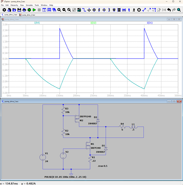
I am working on servicing a circuit board that is used in a Medical Dental sterilizer. The circuit boards used in this model of sterilizer seem to have a chronic problem with a circuit that drives a reciprocating water pump. Here is a schematic of the circuit that fails:

image

My question is what is the advantage to using this circuit configuaration to drive the pump? The gate of the N CH MOSFET turns on and pulls one leg of the load to the negative rail and also turns on the P CH MOSFET about 20 microseconds later pulling the other leg of the load up to the positive rail. While this seems to work quite well it seems to me to be an added complication to be switching both legs of the load. I am hoping for some insight into what the advantage might be in using this configuaration. The Rds (on) of the N CH is about 60 milli Ohm and the Rds of the P CH is about 13 milli Ohm. While I am not certain this is probably a Pulsed circuit as I suspect that the pump needs a Pulsed drive to properly function. My hope is that in better understanding the advantages of this circuit design I might be able to modify it to lower the present failure rate. Failure is usually a shorted P CH Mosfet, A Heat Destroyed N CH MOSFET and a Shorted D26 Diode.

Any insights you may have will be appreciated.

John

  • Sign in to reply
  • Cancel

Top Replies

  • michaelkellett
    michaelkellett 20 days ago in reply to jw0752 +2
    Well, the circuit looks a bit weird - I can only think that it has evolved. On similar things I have wanted to protect the load against the low side MOSFET failing short circuit and added a high side…
  • jw0752
    jw0752 19 days ago in reply to Jan Cumps +2
    Hi Jan, How have you been? I can't tell you how happy it makes me to see so many of the old gang still together.
  • Jan Cumps
    Jan Cumps 20 days ago +1
    Is it possible that the fragile gate of G17 sees too much high (inductive generated) voltage, from motor via R103 and R100, when the motor switches off? Maybe hang an isolated scope between drain and gate…
  • jw0752
    0 jw0752 19 days ago in reply to Jan Cumps

    Hi Jan,

    How have you been? I can't tell you how happy it makes me to see so many of the old gang still together.

    • Cancel
    • Vote Up +2 Vote Down
    • Sign in to reply
    • Verify Answer
    • Cancel
  • jw0752
    0 jw0752 19 days ago in reply to genebren

    Hi Gene,

    Thanks for searching the switching circuits for me. I have never seen this configuration before and when ones skill level is as low as mine the first thought is that the designer had some omnicient insight that is beyond me. I find Michael's suggestion that this is a design that has evolved from its original intention fascinating. When circuits are on high quality circuit boards in very expensive equipment the thought that they may be jury rigged from previous designs didn't occur to me.

    • Cancel
    • Vote Up 0 Vote Down
    • Sign in to reply
    • Verify Answer
    • Cancel
  • jw0752
    0 jw0752 19 days ago in reply to dougw

    Hi Doug,

    Sorry I haven't been around. I have missed you guys. It is hard to explain how life pulls us around and sends us down different paths.

    When I get the boards the D26 is shorted as is the Q17. The Q15 has suffered heat damage to the extent that it may be exploded. It would be relativey easy to put a snubber diode across the load and I may try that on the next board that comes in. Can you think of any scenario where the snubber diode would cause an undesirable side effect? I will not likely get any feedback. If it solves the problem I will just never see the board again. That would be good but it wouldn't satisfy my curiousity. Thank you for your help.

    • Cancel
    • Vote Up 0 Vote Down
    • Sign in to reply
    • Verify Answer
    • Cancel
  • dougw
    0 dougw 19 days ago in reply to jw0752

    If D26 is shorted and Q15 turns on, Q15 will see a large destructive current.

    The snubber diodes, like D26, need to be large enough to handle repeated inductive spikes. It Q15 is driven with some sort of PWM, there will be a lot of inductive spikes, which could add up to absorption of significant energy.

    • Cancel
    • Vote Up +1 Vote Down
    • Sign in to reply
    • Verify Answer
    • Cancel
  • michaelkellett
    0 michaelkellett 19 days ago in reply to jw0752

    I made a mistake in the connection of D1.

    This is a better simulation (with the right circuit, similar diodes to yours for D1 and D2, possibly better values for the load).

    image

    The currents in D1 and D2 are identical which is why you can only see I(D1).

    By adjusting the timing you can set the peak diode currents to Vsupply/Load R.

    D1 and D2 are rated at 1A, Q15 is a protected MOSFET and should be fine with 4A continuous current. Q17 can handle a lot more current.

    It looks as if the diodes are the weakest link but what they actually see depends on the timing, supply voltage and load parameters.

    LTspice is free - I can send the model if you would like it.

    MK

    • Cancel
    • Vote Up +1 Vote Down
    • Sign in to reply
    • Verify Answer
    • Cancel
  • jw0752
    0 jw0752 19 days ago in reply to michaelkellett

    Thanks Michael for taking the time to further investigate. I have the LT Spice program and I would welcome your model so I can play with it myself. 

    • Cancel
    • Vote Up 0 Vote Down
    • Sign in to reply
    • Verify Answer
    • Cancel
  • jw0752
    0 jw0752 19 days ago in reply to dougw

    I will look into the possibility of upsizing the snubber diodes.

    thanks

    • Cancel
    • Vote Up 0 Vote Down
    • Sign in to reply
    • Verify Answer
    • Cancel
  • jc2048
    0 jc2048 19 days ago in reply to jw0752

    Hello John,

    I would think that the designer was familiar with this converter topology

    https://www.vishay.com/docs/91616/twoswitch.pdf

    In the case of the forward converter with a transformer, it guarantees the magnetic reset of the core (with PWM less than 50%), stopping it stepping to saturation, and has a small benefit in recycling much of the magnetizing and leakage energy back to the supply (and thereby lowering the dissipation in the 'snubber' components). I suppose those might also be of benefit with PWM-ing a solenoid, but it's not an area I'm familiar with.

    Are you sure there is no other connection to the top of what looks like it has to be a current-sense resistor (the 0.22R)?

    • Cancel
    • Vote Up +1 Vote Down
    • Sign in to reply
    • Verify Answer
    • Cancel
  • michaelkellett
    0 michaelkellett 19 days ago in reply to jw0752

    LTSpice file here:

    https://www.dropbox.com/scl/fo/876wu0j1vuus2e9t4yz0k/ABlNGiq6fHZOnWuOwdkZHkI?rlkey=9rs366j5r73tu3lft7f4a8rgg&dl=0

    MK

    • Cancel
    • Vote Up 0 Vote Down
    • Sign in to reply
    • Verify Answer
    • Cancel
  • DAB
    0 DAB 17 days ago

    Hi John,

    I am glad you are back.

    I hope you are doing well.

    • Cancel
    • Vote Up 0 Vote Down
    • Sign in to reply
    • Verify Answer
    • Cancel
<>
element14 Community

element14 is the first online community specifically for engineers. Connect with your peers and get expert answers to your questions.

  • Members
  • Learn
  • Technologies
  • Challenges & Projects
  • Products
  • Store
  • About Us
  • Feedback & Support
  • FAQs
  • Terms of Use
  • Privacy Policy
  • Legal and Copyright Notices
  • Sitemap
  • Cookies

An Avnet Company © 2025 Premier Farnell Limited. All Rights Reserved.

Premier Farnell Ltd, registered in England and Wales (no 00876412), registered office: Farnell House, Forge Lane, Leeds LS12 2NE.

ICP 备案号 10220084.

Follow element14

  • X
  • Facebook
  • linkedin
  • YouTube