


Table of Contents
Introduction
Thanks to the productive KiCad time at Xmas with fellow element14 members helping work through understanding KiCAD 6.0, I've put together a video. It is a lot longer (50 minutes) than I wished, so I wasn't happy about that however it is all split into 30 clickable segments (there is a chapter list in YouTube), so at least the average is 90 seconds per topic I guess.. This might be better than 30 separate videos anyway since then there's the risk of a YouTube advert with each one.
Video Contents
Click to jump to the appropriate section:
00:00 - Start 00:27 - KiCad Control Panel 00:59 - Schematic Editor 01:12 - Preferences Configuration for Schematics 01:59 - Schematic Editor Shortcut Keys 02:27 - Schematic Editor Basic Usage 07:22 - Component Symbol Editor 08:29 - Component Symbol Editor 15:33 - Component Footprint Editor 22:03 - Shaped Pads 24:09 - Through-Hole Pads 24:38 - Plated Through-Hole Slots 25:14 - Shaped (Routed) Cuts or Holes 26:58 - Holes (Non-Plated-Through) 28:11 - Schematic Electrical Rules Check 29:10 - PCB Editor 33:38 - Shortcut Keys 37:29 - PCB Design Rules (Constraints) 37:40 - JLCPCB Design Rule Settings 37:49 - Copper Pours and Ground Planes 38:52 - Track Length Tuning 40:53 - Iterative PCB Layout Improvements 41:48 - Via Stitching 42:03 - Removing Solder Resist 42:27 - Checking for Unrouted Nets 42:37 - Running the PCB Design Rules Checker 44:01 - 3D Viewer 44:37 - Generating Gerber Files (CAM Files) 45:25 - JLCPCB Gerber File Settings 47:08 - Gerber Viewer 49:02 - Preparing the Zip File for the PCB Manufacturer 49:16 - Getting Help and Contributing
Naturally, it is still missing a lot (and totally missing everything on Python programmability and 2D/3D CAD) and, not all the content may be best practice, or I may have chosen longer/inefficient ways to do things, but this video is just an option to perhaps save newcomers a few hours hunting around for initial bits of info to get started.
Video:
PCB Editor Configuration Screenshots
Here are screenshots of some of the important configuration windows in KiCad:
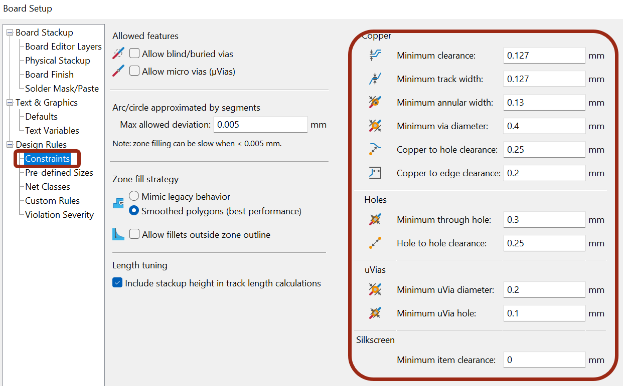
File->Board Setup->Design Rules->Constraints
The settings here are for JLC PCB:
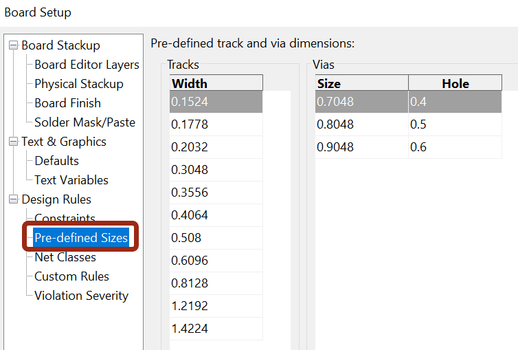
File->Board Setup->Design Rules->Pre-defined Sizes
The settings here are convenient for tracks and vias:
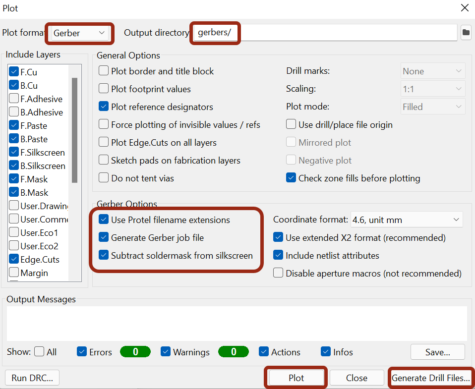
File->Plot
The settings here are suitable for JLC PCB:
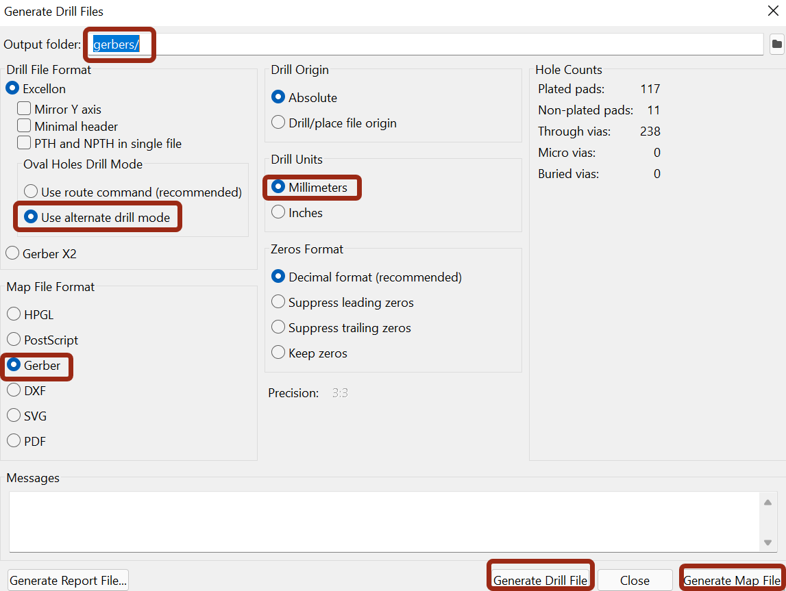
File->Plot->Generate Drill Files
The settings here are suitable for JLC PCB:
Creating Multi-Element Symbols
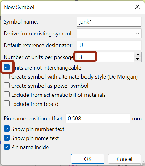
The video is missing this information, but it's useful so it is described here. Sometimes there is a need to have separate symbols for different bits of functionality within the same device. An example would be a quad logic gate, or a DPDT relay where the coil, and the two poles are better represented as separate symbols. The procedure to have these separate sub-symbols is straightforward, it is just a slight modification to the symbol creation method already described in the video.
When creating a symbol, enter the number of units (i.e. sub-symbols), and check the box shown if each of the sub-symbols have fixed pins that cannot be swapped (this will normally be the case, i.e. you will want to check that box):
The symbol editor will now have a Unit box at the top:
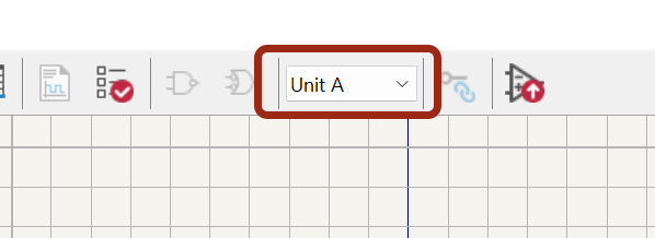
Draw your first sub-symbol, and then select Unit B from that top drop-down box, and draw the next one, and so on. You can copy-paste from one unit to another, or from any symbol into your unit, so that can speed things up when creating and editing symbols.
Use File -> Symbol Properties and set the Footprint parameter to a default existing one if you wish.
Finally, click on Inspect -> Symbol Checker to confirm there’s no issue with the symbol.
Press Ctrl-S to save the footprint.

