element14 Community
element14 Community
    Register Log In
  • Site
  • Search
  • Log In Register
  • Community Hub
    Community Hub
    • What's New on element14
    • Feedback and Support
    • Benefits of Membership
    • Personal Blogs
    • Members Area
    • Achievement Levels
  • Learn
    Learn
    • Ask an Expert
    • eBooks
    • element14 presents
    • Learning Center
    • Tech Spotlight
    • STEM Academy
    • Webinars, Training and Events
    • Learning Groups
  • Technologies
    Technologies
    • 3D Printing
    • FPGA
    • Industrial Automation
    • Internet of Things
    • Power & Energy
    • Sensors
    • Technology Groups
  • Challenges & Projects
    Challenges & Projects
    • Design Challenges
    • element14 presents Projects
    • Project14
    • Arduino Projects
    • Raspberry Pi Projects
    • Project Groups
  • Products
    Products
    • Arduino
    • Avnet Boards Community
    • Dev Tools
    • Manufacturers
    • Multicomp Pro
    • Product Groups
    • Raspberry Pi
    • RoadTests & Reviews
  • Store
    Store
    • Visit Your Store
    • Choose another store...
      • Europe
      •  Austria (German)
      •  Belgium (Dutch, French)
      •  Bulgaria (Bulgarian)
      •  Czech Republic (Czech)
      •  Denmark (Danish)
      •  Estonia (Estonian)
      •  Finland (Finnish)
      •  France (French)
      •  Germany (German)
      •  Hungary (Hungarian)
      •  Ireland
      •  Israel
      •  Italy (Italian)
      •  Latvia (Latvian)
      •  
      •  Lithuania (Lithuanian)
      •  Netherlands (Dutch)
      •  Norway (Norwegian)
      •  Poland (Polish)
      •  Portugal (Portuguese)
      •  Romania (Romanian)
      •  Russia (Russian)
      •  Slovakia (Slovak)
      •  Slovenia (Slovenian)
      •  Spain (Spanish)
      •  Sweden (Swedish)
      •  Switzerland(German, French)
      •  Turkey (Turkish)
      •  United Kingdom
      • Asia Pacific
      •  Australia
      •  China
      •  Hong Kong
      •  India
      •  Korea (Korean)
      •  Malaysia
      •  New Zealand
      •  Philippines
      •  Singapore
      •  Taiwan
      •  Thailand (Thai)
      • Americas
      •  Brazil (Portuguese)
      •  Canada
      •  Mexico (Spanish)
      •  United States
      Can't find the country/region you're looking for? Visit our export site or find a local distributor.
  • Translate
  • Profile
  • Settings
Open Source Hardware
  • Technologies
  • More
Open Source Hardware
Blog Vintage Curvy PCB Traces with KiCad 7
  • Blog
  • Forum
  • Documents
  • Events
  • Polls
  • Members
  • Mentions
  • Sub-Groups
  • Tags
  • More
  • Cancel
  • New
Join Open Source Hardware to participate - click to join for free!
  • Share
  • More
  • Cancel
Group Actions
  • Group RSS
  • More
  • Cancel
Engagement
  • Author Author: shabaz
  • Date Created: 3 Jul 2023 11:43 PM Date Created
  • Views 7164 views
  • Likes 10 likes
  • Comments 32 comments
  • kicad 7
  • kicad 6
  • kicad
Related
Recommended

Vintage Curvy PCB Traces with KiCad 7

shabaz
shabaz
3 Jul 2023
Vintage Curvy PCB Traces with KiCad 7

Table of Contents

  • Introduction
  • What’s Required?
  • Running the Plugin
  • Fixing Issues
  • Summary

Introduction

Old-school printed circuit boards (PCBs) often had wavy copper traces! They were done manually by rolling out UV-light-blocking crepe sticky-backed tape onto clear film.

image

The photo above shows a layout I did as a teenager (I wasn't very good at it). It's for a lighting control unit.

I have meant to experiment with a particular rounded-track feature for KiCad 7 for ages. It ought to produce a reasonable likeness to those old vintage circuit boards! I gave it a shot today. It can transform machine-generated PCB tracks to look more like hand-taped PCB layouts.

What’s Required?

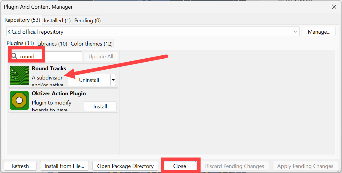
The only prerequisite is to complete your board design (you can still edit it later) and install a special plugin. To install the plugin, on the KiCad startup screen, click on the icon for the Plugin and Content Manager:

image

Search for the Round Tracks plugin, click on it, and install it:

image


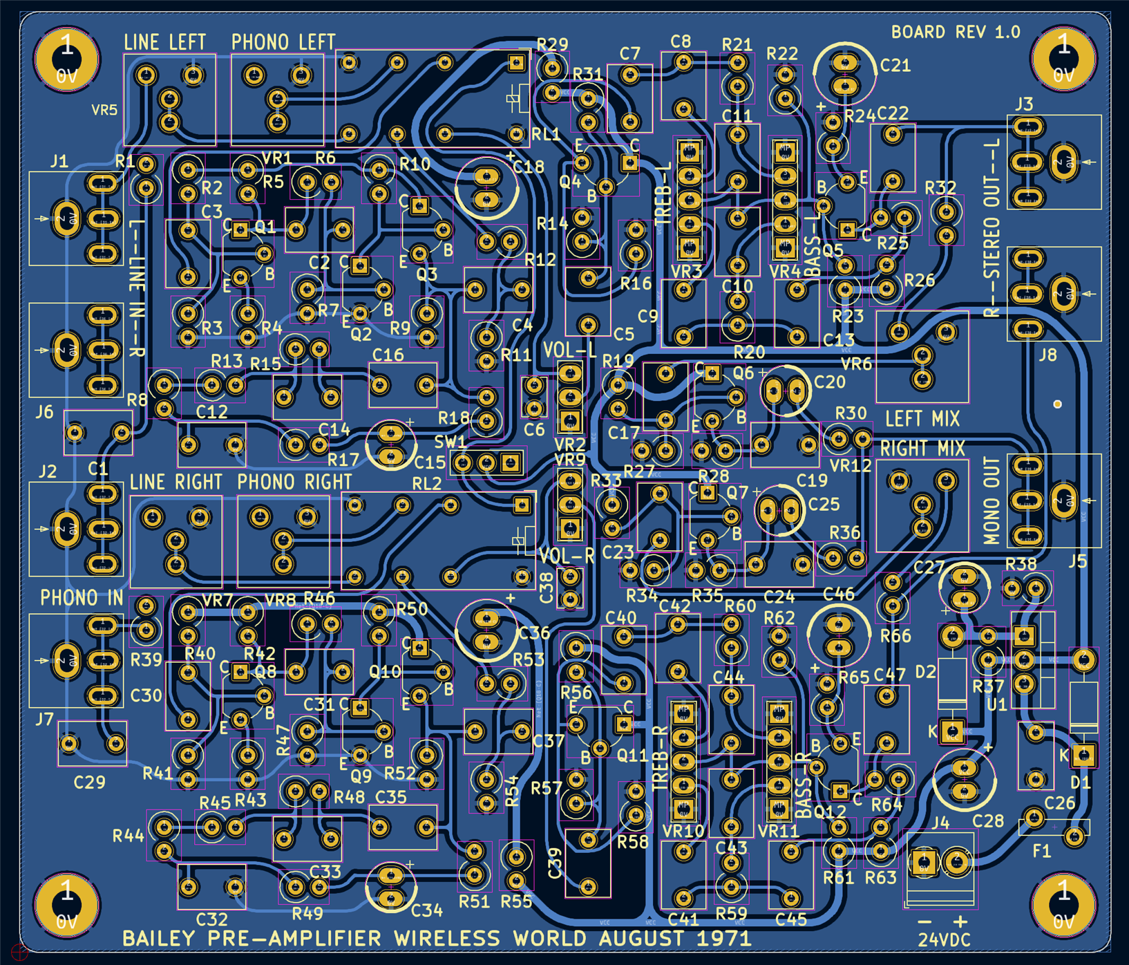
Now open up the PCB Editor for the project you’re working on. In my case, it was an amplifier board:

image

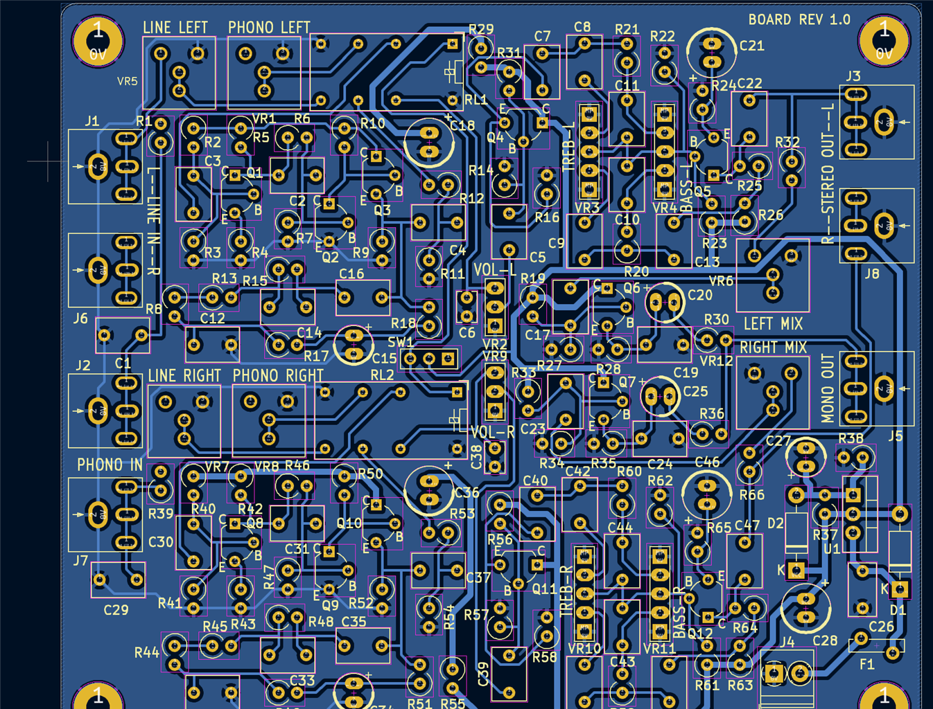
As you can see in the screenshot above, the board is already routed, but using sharp corners on the PCB tracks everywhere.

Running the Plugin

In the PCB Editor, click Tools->External Plugins->Round Tracks. A small settings window will appear. The screenshot below shows what settings I used; there’s not a lot there to configure!

image

Click on Run, and it shouldn’t take too long to execute:

image

Click on OK, and then the new board layout will appear!

Fixing Issues

When you run the Design Rule Check (DRC), some new errors may be revealed. For instance, I had four errors with this board. The first one is highlighted here:

image

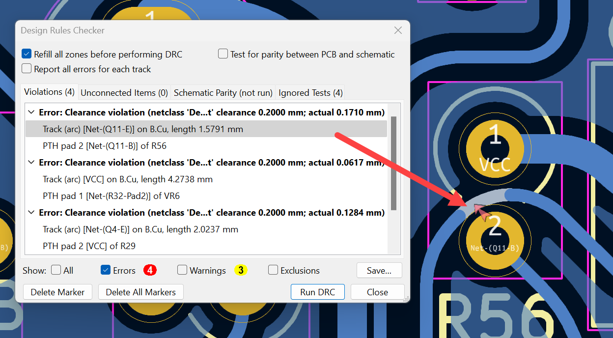
This was easy to fix by closing the newly generated board and editing the original board layout:

image

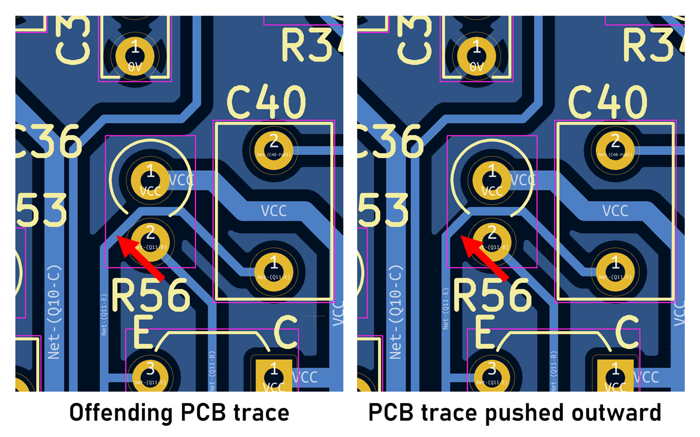
The plugin was re-run, and as seen in the screenshot below, the problem was sorted!

image

All four errors were similar and fixed using the same method.

image


Generally, I think it did a fantastic job, although a few cosmetic artifacts could be tweaked. For instance, a kind of delta shape is visible at the top-right in the screenshot above that could be cleaned up simply by deleting any redundant traces in the generated output.

The new PCB layout will be in a file with a new name (with a -rounded suffix) if the Create a new file option was checked in earlier settings.

Here’s the final error-free result, with most of the redundant traces removed:

image

I think it's not bad, although to keep it 1970s style, it shouldn't have copper fill (or at least, not so tidy copper fill) around the traces!


Summary

Curved vintage-style PCB traces is quite a niche thing to want to do, but it could be interesting, especially for restoring or recreating old electronic products or perhaps retrofitting new functions or interfaces. With KiCad, it was straightforward to do, using a Round Tracks plugin and executing it against a normally-completed PCB design.

The plugin generated a new PCB file, so it is possible to edit the original PCB layout and re-run the plugin as desired, to improve it and resolve any clearance issues caused by rounding tracks too close to other PCB elements.

With KiCad 7, some extra things could be done to improve the look further. For instance, the silkscreen font can be changed to any arbitrary old font (although silkscreen was less common on early boards).

Thanks for reading!

  • Sign in to reply
  • shabaz
    shabaz over 2 years ago in reply to shabaz

    Just saw the fifth one in the photo there is claimed as high as 231.. 

    • Cancel
    • Vote Up 0 Vote Down
    • Sign in to reply
    • More
    • Cancel
  • shabaz
    shabaz over 2 years ago in reply to genebren

    I was just peeking at ebay, to see what the current prices are. The gain values seem to be varying wildly, perhaps that's expected, but I'm surprised some are as high as 193. Anyway, I have no idea, since I know almost nothing about Germanium transistors any more : ( 

    image

    • Cancel
    • Vote Up 0 Vote Down
    • Sign in to reply
    • More
    • Cancel
  • genebren
    genebren over 2 years ago in reply to shabaz

    I do see a lot of eBay listings for both germanium transistors and diodes, some with reasonable pricing.  I have been looking for some for some synthesizer projects for a while.

    • Cancel
    • Vote Up 0 Vote Down
    • Sign in to reply
    • More
    • Cancel
  • shabaz
    shabaz over 2 years ago in reply to jc2048

    Interesting. I'm going to get one to compare with the OA47!

    • Cancel
    • Vote Up 0 Vote Down
    • Sign in to reply
    • More
    • Cancel
  • jc2048
    jc2048 over 2 years ago in reply to shabaz

    It must be a modern equivalent to the 1N270: the datasheet says it's not a point-contact diode.

    • Cancel
    • Vote Up 0 Vote Down
    • Sign in to reply
    • More
    • Cancel
>
element14 Community

element14 is the first online community specifically for engineers. Connect with your peers and get expert answers to your questions.

  • Members
  • Learn
  • Technologies
  • Challenges & Projects
  • Products
  • Store
  • About Us
  • Feedback & Support
  • FAQs
  • Terms of Use
  • Privacy Policy
  • Legal and Copyright Notices
  • Sitemap
  • Cookies

An Avnet Company © 2025 Premier Farnell Limited. All Rights Reserved.

Premier Farnell Ltd, registered in England and Wales (no 00876412), registered office: Farnell House, Forge Lane, Leeds LS12 2NE.

ICP 备案号 10220084.

Follow element14

  • X
  • Facebook
  • linkedin
  • YouTube