element14 Community
element14 Community
    Register Log In
  • Site
  • Search
  • Log In Register
  • Community Hub
    Community Hub
    • What's New on element14
    • Feedback and Support
    • Benefits of Membership
    • Personal Blogs
    • Members Area
    • Achievement Levels
  • Learn
    Learn
    • Ask an Expert
    • eBooks
    • element14 presents
    • Learning Center
    • Tech Spotlight
    • STEM Academy
    • Webinars, Training and Events
    • Learning Groups
  • Technologies
    Technologies
    • 3D Printing
    • FPGA
    • Industrial Automation
    • Internet of Things
    • Power & Energy
    • Sensors
    • Technology Groups
  • Challenges & Projects
    Challenges & Projects
    • Design Challenges
    • element14 presents Projects
    • Project14
    • Arduino Projects
    • Raspberry Pi Projects
    • Project Groups
  • Products
    Products
    • Arduino
    • Avnet & Tria Boards Community
    • Dev Tools
    • Manufacturers
    • Multicomp Pro
    • Product Groups
    • Raspberry Pi
    • RoadTests & Reviews
  • About Us
    About the element14 Community
  • Store
    Store
    • Visit Your Store
    • Choose another store...
      • Europe
      •  Austria (German)
      •  Belgium (Dutch, French)
      •  Bulgaria (Bulgarian)
      •  Czech Republic (Czech)
      •  Denmark (Danish)
      •  Estonia (Estonian)
      •  Finland (Finnish)
      •  France (French)
      •  Germany (German)
      •  Hungary (Hungarian)
      •  Ireland
      •  Israel
      •  Italy (Italian)
      •  Latvia (Latvian)
      •  
      •  Lithuania (Lithuanian)
      •  Netherlands (Dutch)
      •  Norway (Norwegian)
      •  Poland (Polish)
      •  Portugal (Portuguese)
      •  Romania (Romanian)
      •  Russia (Russian)
      •  Slovakia (Slovak)
      •  Slovenia (Slovenian)
      •  Spain (Spanish)
      •  Sweden (Swedish)
      •  Switzerland(German, French)
      •  Turkey (Turkish)
      •  United Kingdom
      • Asia Pacific
      •  Australia
      •  China
      •  Hong Kong
      •  India
      •  Japan
      •  Korea (Korean)
      •  Malaysia
      •  New Zealand
      •  Philippines
      •  Singapore
      •  Taiwan
      •  Thailand (Thai)
      •  Vietnam
      • Americas
      •  Brazil (Portuguese)
      •  Canada
      •  Mexico (Spanish)
      •  United States
      Can't find the country/region you're looking for? Visit our export site or find a local distributor.
  • Translate
  • Profile
  • Settings
Open Source Hardware
  • Technologies
  • More
Open Source Hardware
Forum Making pcbs
  • Blog
  • Forum
  • Documents
  • Events
  • Polls
  • Members
  • Mentions
  • Sub-Groups
  • Tags
  • More
  • Cancel
  • New
Join Open Source Hardware to participate - click to join for free!
Actions
  • Share
  • More
  • Cancel
Forum Thread Details
  • Replies 24 replies
  • Subscribers 323 subscribers
  • Views 3524 views
  • Users 0 members are here
  • raspberry
  • toner
  • hydrogen
  • pi
  • peroxide
  • chloride
  • copper
  • pcb
  • hydrochloric
  • acid
  • ferric
  • arduino
Related

Making pcbs

terrydark
terrydark over 11 years ago

Hi everyone,


This is my first discussion but I would like to see what the consensus is using  the knowledge and experience of all that have manufactured their own boards using "home brew" techniques.


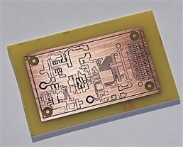
In in your opinion, what is the best or perhaps economical and least fiddly of the methods for producing pcb boards via DIY?


Thanks in advance


Terry

  • Sign in to reply
  • Cancel

Top Replies

  • michaelkellett
    michaelkellett over 11 years ago +1
    As far as I know there is no convenient or free legal way of disposing of the waste products from etching copper from boards. In my youth (alas distant, early 1970s) I poured it down the drain but I understand…
  • D_Hersey
    D_Hersey over 11 years ago in reply to michaelkellett +1
    I have a set-up in my garage. Agitated ferric-chloride bath, tin plating, wet saw, ventilated drill press, xytable. I have a thermal press that directly transfers stencils from a laser-printer. Haven't…
  • johnbeetem
    johnbeetem over 11 years ago in reply to D_Hersey +1
    Don Hersey wrote: Another technique is to buy generic PCBs and modify them. The 'op-amp evaluation boards' from the few remaining linear players are better than I can make. Ebay ones from China for…
Parents
  • D_Hersey
    D_Hersey over 11 years ago

    I buy directly from the manufacturer because I am concerned more about freshness and quality than price-point.  I cannot imagine a scenario in which a sheet of PnP blue is going to figure significantly into the total effort.


    Home


    Their press if pricey, but it has worked well for me and seems to be of stout manufacture.

    • Cancel
    • Vote Up +1 Vote Down
    • Sign in to reply
    • Cancel
  • terrydark
    terrydark over 11 years ago in reply to D_Hersey

    Way better pricing on the press n peel - I will give this a try too.  Thanks.


    The press is a bit pricey - It looks a bit like a t-shirt press... or is it?  Fran Blanche used a similar press in her video.


    The PCB materials look OK - do you buy from here too?


    Have you used any photosensitive resist pcbs?  The boards here at the local electronics store are $5.95 for single sided positive resist 114mm x 165mm (4.5" x 6.5")


    Finishing? Solder mask?  layout?


    Thanks for your great input, by the way. Everyone has been very helpful.


    With regards to you earlier comment "PCB milling plus hole collars is the way to go nowadays if one insists" can you describe your process if you don't mind? Is your mill an expensive one?  Any idea of running cost? Any info would be great.  Are hole collars what they sound like ie an aid to implement double sided boards?  Excuse my ignorance... I have skipped over DIY PCB making by going the out sourced route and I am ignorant to many aspects of DIY PCB to my regret.


    Regards


    Terry

    • Cancel
    • Vote Up 0 Vote Down
    • Sign in to reply
    • Cancel
  • D_Hersey
    D_Hersey over 11 years ago in reply to terrydark

    Glad to be of service to you sir--good luck in your endeavors!


    Everyone has their preferred method of PCB fab.  Every time we add a layer of complexity, we open the door to problems, I think.  In psychology we know that some seek complexity for its own sake, perhaps as a refuge.  They are said to be in a 'perfectionistic regress.'  One of the things we seem to monitor in e- is our own mentalities.  Just trying to say that the more we try to do everything, the more we are exposing ourselves to hidden costs.  Some years back, my son was etching, went to check its progress in the garage, and made the mistake of taking his safety glasses off before shutting off the lights.  Inexplicably, he pivoted around in turning off the lights and a drop of etchant, propelled by the aerator, happened into his eye. This was rather a fluke, he was steps away from the unit, musta been a perfect storm.  We washed out his eye in the sink and sent him to the hospital, which by the grace of the almighty is right down the street.  He was okay, but the experience was upsetting to his mother and myself.


    You can use photo-resist, I have, it works, in some cases the developer is diluted lye, which isn't too bad, but represents one more problem.  My finding was that I was generating the artwork by laser-printing on acetate in the first place, so using photography in the process seemed to be an extra layer of complexity for which I could not divine any reward.  But that is just my opinion.  Buying the pre-coated boards was expensive, coating them myself was a hassle.  I don't, myself, use the cheapest foreign board houses.  Using high quality on-shore providers assures me that they are probably not major polluters.  They etch with 10% nitric acid which they recycle.  They recover the copper.  The problem with dumping copper down the sewer, not that I am accusing you of planning that, is that it is a nutrient.  Bio-films bloom and clog the pipes.  I know the workers are protected because they use closed-cycle machines.  IMHO, the photo method is more appropriate for hand-made artwork on acetates, using ink and tape and lith-film, a method most were happy to dispense with upon the maturation of computer graphics as a technique to achieve this purpose.  Optimally, one uses a vacuum-frame for the exposure, expensive.  Then you will end up with some kind of actinic light set-up to clutter up your garage when you just want to retrieve a grill or basketball.


    As far as milling goes, the machine is expensive, and if I owned one, its duty-cycle would be low.  If I knew lotsa well-heeled interested parties in my vicinity, it would be cool to own part of one as part of a collective.  Some people are working to have equipment such as this associated with public libraries, a movement I applaud: clap, clap, clap!!!


    After you etch, often you must drill.  Most PCBs are fabricated from fiberglass-epoxy.  Make sure to set up a little vacuum cleaner nozzle C-clamped to your drill-press table to suck up the dust.  I have a small wet-saw to part my boards, using a shear would probably be cleaner.  Vector corp, IIRC sells these little sleeves that make it like you have plated-thru holes.  Small carbide drills for PCB work are brittle, expensive and short-lived.  They cannot handle the stress of use in a regular drill-press, one has to employ either a small one, or use a special adapter from a tool-house.


    Routine accounting practices attach a high cost to business for each line-item they inventory.  You could wind up with all of this stuff.  I live in a relatively chi-chi semi-urban neighborhood.  It is hard for any enterprise to justify the ground it sits on, around here.  If you have plenty of space, not so much of a problem.  I have about ten thousand dollars worth of metal drawer-cabinets for my stuff.  Much of my inventory is in a state of semi-obsolescence.  Alas!  In for a penny, in for a pound.

    • Cancel
    • Vote Up 0 Vote Down
    • Sign in to reply
    • Cancel
  • Kilohercas
    Kilohercas over 11 years ago in reply to D_Hersey

    how about this level of home made pcb ?


         imageimageimage

    Simple UV technology, with good mask, and dynamask for soldermask. works just fine, but lot of work. Now i switched to OSH Park

    • Cancel
    • Vote Up 0 Vote Down
    • Sign in to reply
    • Cancel
Reply
  • Kilohercas
    Kilohercas over 11 years ago in reply to D_Hersey

    how about this level of home made pcb ?


         imageimageimage

    Simple UV technology, with good mask, and dynamask for soldermask. works just fine, but lot of work. Now i switched to OSH Park

    • Cancel
    • Vote Up 0 Vote Down
    • Sign in to reply
    • Cancel
Children
  • terrydark
    terrydark over 11 years ago in reply to Kilohercas

    Any details on the technologies you used?


    UV I know - I used to use it for curing certain lacquers and paints.


    dyna mask - what exactly is this and how is it used?


    Thanks


    Terry

    • Cancel
    • Vote Up 0 Vote Down
    • Sign in to reply
    • Cancel
  • Kilohercas
    Kilohercas over 11 years ago in reply to terrydark

    Simple UV photo-resist + mask. The trick is to get very high quality mask, and double it. print only in black, no other colors (give better edge) I go into press and they use large industrial Xerox printer, not some Laserjet from HP


    Dynamask can buy from ebay, info could be found in google. Again, trick to get good soldermask is to use double or tripple mask, for same high quality printer. 1minute UV expose for dynamask, and 4 for Photoresist. Etching is in FeCl3

    • Cancel
    • Vote Up 0 Vote Down
    • Sign in to reply
    • Cancel
  • terrydark
    terrydark over 11 years ago in reply to Kilohercas

    Thanks for the info, Linas


    I will see if I can get hold of some DynaMask if I take the DIY path


    Regards


    Terry

    • Cancel
    • Vote Up 0 Vote Down
    • Sign in to reply
    • Cancel
element14 Community

element14 is the first online community specifically for engineers. Connect with your peers and get expert answers to your questions.

  • Members
  • Learn
  • Technologies
  • Challenges & Projects
  • Products
  • Store
  • About Us
  • Feedback & Support
  • FAQs
  • Terms of Use
  • Privacy Policy
  • Legal and Copyright Notices
  • Sitemap
  • Cookies

An Avnet Company © 2026 Premier Farnell Limited. All Rights Reserved.

Premier Farnell Ltd, registered in England and Wales (no 00876412), registered office: Farnell House, Forge Lane, Leeds LS12 2NE.

ICP 备案号 10220084.

Follow element14

  • X
  • Facebook
  • linkedin
  • YouTube