


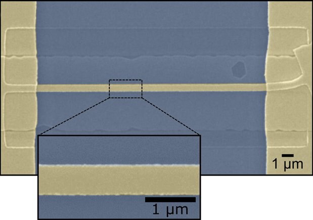
An image taken by a scanning electron microscope reveals a single-crystal gold nanowire on a thermal oxide substrate. (Image Credit: Natelson Research at GroupRice University)
Utilizing an advanced optical detection system, researchers at Rice University have discovered that electricity generated from temperature differences isn’t affected by grain boundaries positioned in its way in nanoscale gold wires. However, this thermoelectric response can be altered by strain and other defects in the material. This phenomenon could potentially detect crystalline defects in conducting materials that are otherwise difficult to find with advanced microscopes. The researchers published their findings in the Proceedings in the National Academy of Sciences on September 22, 2020.
"A lot of times, people think about the thermoelectric effect when they're building solar panels or generating power from this or that," doctoral alumni Charlotte Evans said. "We argue instead that the thermoelectric effect is a really interesting diagnostic tool."
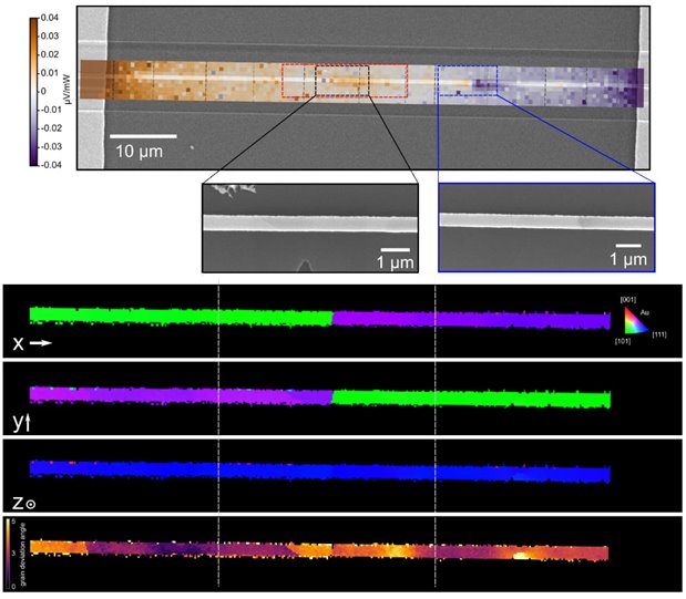 This optical detection system shows defects in a gold nanowire that may otherwise seem like it’s a perfect crystal under a scanning electron microscope. (Image Credit: Charlotte Evans/Rice University)
Grain boundaries are planes in materials where misaligned crystals gather, causing atoms along the edge to adjust while binding to their neighbors. Measurements in bi-crystal gold nanowires created by Jonathon Fan, an electrical engineer at Stanford University, revealed that there is no detectable effect on thermoelectric voltages at the grain boundary. Instead, the electrons ignored the individual grain boundary.
Temperature differences in conductors produce thermoelectricity via a type of thermoelectric effect known as the Seebeck effect. Temperature differences are frequently measured by using this effect, which can also control thermostats. The researchers set off the Seebeck effect by heating a part of Fan’s nanowires with a highly controlled laser. This caused electrons to transfer from the heated area to colder parts and produced a measurable voltage. When the laser moved across the grain boundary in the crystals, it revealed that there was no measurable change in the voltage.
Changes in the voltage were evident when the laser was moved across portions of the nanowires that were deformed, which included distortions in the crystal lattice throughout the wire. The defects were partially repaired by strengthening the distorted devices, which resulted in more obvious changes in the thermoelectric current
"There's a community of people who play around with improving thermoelectric response," Rice physicist Doug Natelson said. "They need to be aware that structural issues like very small distortions to the lattice have effects that are not necessarily small. People tend to ignore these tiny structural issues, but anytime you're making thin-film devices, there's baked-in stress and strain in the material, just because of the way it's made."
Nanoscale crystals are commonly characterized by an expensive and lengthy process known as electron backscatter diffraction (EBSD). "The benefit of our process is its simplicity," Evans said. "We use a large spot size from a laser, two microns, which is much larger than the size of an e-beam, and we can detect variations using just a lock-in technique, a scanning laser and a voltage amplifier.”
"If you look at the plain EBSD data, it looks as though you have a pristine crystal," she said. "And it's not until you post-process the data and look at how each pixel varies from the next that you would see small distortions along the length of the wire. It's complicated to detect. That's why it's so remarkable that we could detect these little variations with a laser."
"So if you want to do something clever and exploit the thermoelectric response, you need to understand the devices you're making with standard, top-down fabrication methods," Natelson said. "The stress and strain and what seemed like minor structural imperfections can have an easily detectable influence."
Have a story tip? Message me at: cabe(at)element14(dot)com