element14 Community
element14 Community
    Register Log In
  • Site
  • Search
  • Log In Register
  • About Us
  • Community Hub
    Community Hub
    • What's New on element14
    • Feedback and Support
    • Benefits of Membership
    • Personal Blogs
    • Members Area
    • Achievement Levels
  • Learn
    Learn
    • Ask an Expert
    • eBooks
    • element14 presents
    • Learning Center
    • Tech Spotlight
    • STEM Academy
    • Webinars, Training and Events
    • Learning Groups
  • Technologies
    Technologies
    • 3D Printing
    • FPGA
    • Industrial Automation
    • Internet of Things
    • Power & Energy
    • Sensors
    • Technology Groups
  • Challenges & Projects
    Challenges & Projects
    • Design Challenges
    • element14 presents Projects
    • Project14
    • Arduino Projects
    • Raspberry Pi Projects
    • Project Groups
  • Products
    Products
    • Arduino
    • Avnet Boards Community
    • Dev Tools
    • Manufacturers
    • Multicomp Pro
    • Product Groups
    • Raspberry Pi
    • RoadTests & Reviews
  • Store
    Store
    • Visit Your Store
    • Choose another store...
      • Europe
      •  Austria (German)
      •  Belgium (Dutch, French)
      •  Bulgaria (Bulgarian)
      •  Czech Republic (Czech)
      •  Denmark (Danish)
      •  Estonia (Estonian)
      •  Finland (Finnish)
      •  France (French)
      •  Germany (German)
      •  Hungary (Hungarian)
      •  Ireland
      •  Israel
      •  Italy (Italian)
      •  Latvia (Latvian)
      •  
      •  Lithuania (Lithuanian)
      •  Netherlands (Dutch)
      •  Norway (Norwegian)
      •  Poland (Polish)
      •  Portugal (Portuguese)
      •  Romania (Romanian)
      •  Russia (Russian)
      •  Slovakia (Slovak)
      •  Slovenia (Slovenian)
      •  Spain (Spanish)
      •  Sweden (Swedish)
      •  Switzerland(German, French)
      •  Turkey (Turkish)
      •  United Kingdom
      • Asia Pacific
      •  Australia
      •  China
      •  Hong Kong
      •  India
      •  Korea (Korean)
      •  Malaysia
      •  New Zealand
      •  Philippines
      •  Singapore
      •  Taiwan
      •  Thailand (Thai)
      • Americas
      •  Brazil (Portuguese)
      •  Canada
      •  Mexico (Spanish)
      •  United States
      Can't find the country/region you're looking for? Visit our export site or find a local distributor.
  • Translate
  • Profile
  • Settings
Power & Energy
  • Technologies
  • More
Power & Energy
Forum MOSFET recomendation for LTC4008 Li-ion Charger (5 cells pack)
  • Blog
  • Forum
  • Quiz
  • Documents
  • Polls
  • Events
  • Mentions
  • Sub-Groups
  • Tags
  • More
  • Cancel
  • New
Actions
  • Share
  • More
  • Cancel
Forum Thread Details
  • State Verified Answer
  • Replies 13 replies
  • Answers 1 answer
  • Subscribers 286 subscribers
  • Views 1794 views
  • Users 0 members are here
  • mosfet
  • battery
  • charger
Related

MOSFET recomendation for LTC4008 Li-ion Charger (5 cells pack)

Former Member
Former Member over 12 years ago

Hi,


I´m currently designing a 5 cell pack Li-ion charger with LTC4008 chip (discussion posted in Sep 2011 in this thread)

In page 15 of LTC4008 datasheet you can find the topic about the MOSFET selection.


I´m certainly lost in the proper selection. I know that logic-level MOSFETS must be used (gate voltage around (5.6V-6V), but is the first time for me designing with mosfets.


One important point is the output voltage of the carger, datasheet says that if Vout>20V then the RDSon should be little more high for reducing the ripple...


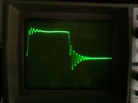
The charge voltage will be 20.5V and maximum Output Current 1.5A


I was thinking on use the mosfets that appear in the schematics of the datasheet, but has anyone any recommendation?, I mean, do I have to go deep in the mosfets area or can I use one recommended by anyone who has be involved in similar scenarios?


The only important thing in this design is the proper selection for minimum ripple current, at cost of something (as always). Efficiency for example is not a problem cause it´s a battery charger (I prefer to lost energy efficency if that means reduce ripple current in the output). I´m thinking to use a slightly high Inductor (around 40 microH) and two low ESR tantalum capacitors "surge robust" in parallel in the output of the mosfets.


Any comments are appreciated


PS: I need reference values. (What means high ... what means low... 0.001 - 0.01 ? (in mosfet parameters)

  • Sign in to reply
  • Cancel
Parents
  • Former Member
    0 Former Member over 12 years ago

    Notes on this thread from LTC factory applications. NOt from me.


    There are a number of misinformed thoughts here in this thread. The issues at hand are a power supply book unto themselves. Here are my responses to the most salient points.


    • The DS does not at all relate the ripple with the RDSon. These are fundamentally different quantities. RDSon is the effective steady-state on-state resistance of a MOSFET. Output (voltage) switching ripple in a PWM circuit is a function of the on/off states of the MOSFET pair in conjunction with the inductor. This voltage pulsing causes the current through the inductor to go up and down in a triangular manner. If this were directly applied to the output, you could have horrible results. Thus it is filtered with the output capacitor. What I believe he is referring to is actually the ESR (equivalent series resistance). This is discussed in pg. 14-15. (The value of the capacitance and voltage rating largely affects the sort of expected ESR range given a specific part family due to the physical construction of the capacitor.) Choose the capacitor appropriately in relationship to the “acceptable” amount of the voltage ripple.


    • I am speaking comparatively here and according to what is being addressed by pg. 16. RDSon is indirectly related to is the switching (or transition) loss, which is a function of many parameters, but gets worse with higher VIN because you must use FETs with higher voltage rating. Two things happen:
      • Increasing the voltage rating and trying to keep a similar RDSon inherently increases the gate charge (Qg) and capacitance (CSS, etc.), both contributing to higher losses.
      • The RDSon goes up (usually) if you try to keep the same Qg relative to the previous choice at the lower voltage rating.

    The only the circuit designer can control is to use a FET with lower Qg and Miller capacitance figures, but therein is the trade-off to higher RDSon. For the same voltage rating of FET, you will have to compromise between lowest RDSon and lowest Qg. This is what relates to the efficiency degradation. In the case of the battery charger, we are mostly concerned with finding the happy medium of minimizing the transition losses and maximizing efficiency hit.


    • The FETs used in the demo circuit are acceptable for use in this app, however I would caution the use of an input voltage too close to the FET rating as the switch node will see switching peaks slightly higher depending on the parasitic trace inductance due to layout. It is small and finite, but there are ways to minimize its effects. The switch node can be snubbed out with an RC circuit, but usually the best bet is to minimize the distance from the FETs to the inductor. Or even simpler & safer, use a 40VD-S rated FET.


    • General FET selection tips:
      • Choose your vendor. This is non-trivial if you have bizarre requirements, but in this case the trickiest component is the top FET, which is a P-channel MOSFET. Vishay and Fairchild have been our choices in the past.
      • Choose according to the maximum voltage they will see. In the case of this design, the input and output voltage exceeds 20, so a 30V should be acceptable. However, intuitively you would know that if the input were at 29V, this would be a marginal situation and so should actually be upped to 40V rating. Judgment and experience will show best what is necessary, but a good PCB layout should not see a large excursion. As my personal rule of thumb, I like to estimate at least a ~5V differential between max rating and the max voltage applied to the circuit. As I said, the peak can actually be a little higher due to trace inductance.
      • Next, choose what is an acceptably rated gate drive according to the switching controller in question. Most LTC parts run a 5V gate drive, which is a common rating. This limits the choices further.
      • Choose the preferred package type. In this case, the design could be accomplished with SO-8 or smaller due to the current levels. There should be no reason to “overdesign” the circuit; it can be costly and has diminishing returns for many other reasons.
      • Among the maybe 5-10 choices remaining from the filtering above, choose one with appropriate current rating. In a buck, the worst-case current is seen by the


    • The customer is correct in observing most people don’t care too much of the efficiency of the circuit. Since this is a buck topology, the efficiency can be expected to be in the low- to mid-90s anyway, assuming decent component choices.
    • As for the # of cells, there is a finite number of combinations you want to allow for in the design of a demoboard for common usage. The stacks used back during its design probably did not go past 4-cells, so to design up to 6 may have been a little difficult while still maintaining one inductor value and a simple battery voltage jumper setting. Since the voltage is actually “continuously adjustable” via resistor, only the min/max limits are really of any concern.
    • As observed towards the end of the discussion (as of 2/11) Q1A prevents the load from back-powering the input of the circuit. It is commonly used in our chargers in this manner. The reason it is P-channel so that it does not need an extra “boost” supply to create a bias higher than the rest of the circuit, which will cost extra current to keep on. Q1B allows an alternative path for the battery to power the load rather than going through the top FET (Q2). When you remove input power Q2 will not switch, but it will still conduct battery current through the intrinsic body diode at a true silicon diode drop, causing power loss proportional to the load current, possibly blowing out the top FET due to excessive power dissipation. When the input is removed, R16 pull hard down on the Q1B gate to turn it on. D2 clamps the voltage from gate to source so that the limits are not exceeded on the FET when the input supply returns. It can be an N-channel too, but then you must derive the gate control as a positive bootstrapped voltage on top of the battery voltage to make Vg>Vs, so it is easily accomplished by a P-channel with no extra switching.
    • If you connect the load to the charger output (“charger-fed”), a load cannot exceed battery charge limit. E.g. a 2A charge current limit could never supply more than 2A to a load demanding more current; the output would simply collapse to 0V if the load impedance was low enough. Somewhere in between would still starve the battery for current, causing the charge time to be extended. The arrangement in the demo circuit allows parallel operation of the load while fully charging the battery, assuming the input current limit has not been reached.
    • Relays in battery charger circuits are a bad idea because they take so long to turn on/off, causing the output of the charger to see a high impedance very quickly. This can cause the energy that was trying to make its way to the battery to temporarily raise the output capacitor voltage beyond the programmed amount. This “boosting” can run through the top FET body diode actually getting sent back to the input.
    • Cancel
    • Vote Up 0 Vote Down
    • Sign in to reply
    • Reject Answer
    • Cancel
  • Former Member
    0 Former Member over 12 years ago in reply to Former Member

    Hi,

    As most of these mofest are obsolete, here goes my choice for a system with:


    DCIN -> 24V

    V(out)charge max -> 20.5V

    I charge max -> 1.5A (slow charge)

    I load max -> 100-200mA


    Q1A: (Named on Demoboard 496B circuit) SO-8


    SQ4431EY -> Automotive P-Channel 30 V (D-S) 175 °C MOSFET


    Reverse Transfer Capacitance Crss [140 - 175] pF

    Total Gate Chargec Qg [25 - 38] nC


    ABSOLUTE MAXIMUM RATINGS (TC = 25 °C, unless otherwise noted)

    Drain-Source Voltage VDS -30V

    Gate-Source Voltage VGS ±20V

    Continuous Drain Current TC = 25 °C Id -10.8A --- TC = 125 °C -6.2A

    Continuous Source Current (Diode Conduction) IS -5.4A

    Maximum Power Dissipation TC = 25 °C PD 6W --- TC = 125 °C 2W


    Q1B:

    Mike, nice trick with R16, Q1B and D2, now it´s clear their pourpose. But as my load will be limited to 200mA (more or less) I thought that Q2 will be happy with the power dissipation, so I´ve removed Q1B.


    Q2: SO-8


    Si4431CDY -> Load Switch/Battery Switch P-Channel 30-V MOSFET


    Reverse Transfer Capacitance Crss 145 pF

    Total Gate Chargec Qg [13 - 38] nC


    ABSOLUTE MAXIMUM RATINGS (TC = 25 °C, unless otherwise noted)

    Drain-Source Voltage VDS -30V

    Gate-Source Voltage VGS ±20V

    Continuous Drain Current Id from -6A to -9A

    Continuous Source Current (Diode Conduction) Is from -2.1A to -3.5A  <---- It should be very comfort for 200mA max (I load)

    Maximum Power Dissipation from 2W to 4W


    I have changed the BGATE mosfet to this one..


    Q7: SO-8


    FDS6612A -> Single N-Channel, Logic-Level, PowerTrench(R) MOSFET


    This N-Channel Logic Level MOSFET is produced using Fairchild Semiconductor’s  advanced PowerTrench process that has been especially tailored to minimize the on-state resistance and yet maintain superior switching performance. These devices are well suited for low voltage and battery powered applications where low in-line power loss and fast switching are required.


    Reverse Transfer Capacitance Crss 55 pF

    Total Gate Chargec Qg [5.4 - 7.6] nC  <---- It´s very nice!


    ABSOLUTE MAXIMUM RATINGS (TC = 25 °C, unless otherwise noted)

    Drain-Source Voltage VDS 30V

    Gate-Source Voltage VGS ±20V

    Continuous Drain Current Id from 8.4A (continuous) to 40A (pulsed)

    Continuous Source Current (Diode Conduction) Is 2.1A

    Maximum Power Dissipation from 1W to 2.5W


    Clearly I have chosen to stay in max Vds 30V. I assume that he ripple in the DCIn of 24V should not be beyond  29-30V.


    As I charge with a low current of 1.5A max, and the batteries are of 4,4A/h, plus the frecuency of charge will be low (two times per month estimated)... those conditions drove me to choose 30Vds max. Because the friendly conditions...if not I would choose 40Vds max.


    Cheers!


    • Cancel
    • Vote Up 0 Vote Down
    • Sign in to reply
    • Verify Answer
    • Cancel
  • Former Member
    0 Former Member over 12 years ago in reply to Former Member

    These are the results for those mosfets after designing the pcb.


    Vout = 20.4V +- 2mV! (Voltage ripple is quite nice)


    I use 68uH inductor (SRR1260-680M) and two 10uF tantalum Surge-robust capacitors in parallel (T495D106K035ATE300)


    One of the power mosfet´s gate in action:


    0.05useg / division

    2V / div


    image


    I appreciate comments about this waveform, I think it seems pretty nice...


    Cheers

    • Cancel
    • Vote Up 0 Vote Down
    • Sign in to reply
    • Verify Answer
    • Cancel
Reply
  • Former Member
    0 Former Member over 12 years ago in reply to Former Member

    These are the results for those mosfets after designing the pcb.


    Vout = 20.4V +- 2mV! (Voltage ripple is quite nice)


    I use 68uH inductor (SRR1260-680M) and two 10uF tantalum Surge-robust capacitors in parallel (T495D106K035ATE300)


    One of the power mosfet´s gate in action:


    0.05useg / division

    2V / div


    image


    I appreciate comments about this waveform, I think it seems pretty nice...


    Cheers

    • Cancel
    • Vote Up 0 Vote Down
    • Sign in to reply
    • Verify Answer
    • Cancel
Children
No Data
element14 Community

element14 is the first online community specifically for engineers. Connect with your peers and get expert answers to your questions.

  • Members
  • Learn
  • Technologies
  • Challenges & Projects
  • Products
  • Store
  • About Us
  • Feedback & Support
  • FAQs
  • Terms of Use
  • Privacy Policy
  • Legal and Copyright Notices
  • Sitemap
  • Cookies

An Avnet Company © 2025 Premier Farnell Limited. All Rights Reserved.

Premier Farnell Ltd, registered in England and Wales (no 00876412), registered office: Farnell House, Forge Lane, Leeds LS12 2NE.

ICP 备案号 10220084.

Follow element14

  • X
  • Facebook
  • linkedin
  • YouTube