Table of Contents
Hi,
I'm having trouble bringing up a circuit and I figured I'd ask here in case anyone can spot where I'm going wrong. I will also raise it with the chip manufacturer and point them to this discussion so that they can see the detail more easily. Unfortunately, there seems to be almost zero information on the Internet about this chip, beyond the datasheet, so I have nothing to compare against.
The Problem:
A USB-C circuit consisting of a DC-DC converter and a USB-C Power Delivery controller isn't functioning as expected. According to the PDF datasheet of the MP5031 USB-C Power Delivery controller chip, the chip has a default configuration, but I need to program via I2C certain register settings so that it functions with the MP2491C DC-DC converter chip I have selected. The I2C registers are supposed to be one-time-programmable (OTP), so if I program them incorrectly, the chip needs to be desoldered and replaced with a new one. I don't mind doing that, but only if I definitely have messed that up.
The specific IC I am using is part code MP5031GRE-00A3-P.
I have programmed the I2C register settings in the manner that I thought was correct. After programming, I read the settings and verified that they were what I expected.
All good so far. However, after I reboot, and re-read the I2C registers, the settings are back to the defaults!
There is this snippet in the datasheet:
"These registers are one-time programmable (OTP). If the MP5031’s VCC voltage (VCC) exceeds the UVLO rising threshold, then the OTP items are loaded to the I2C register."
I have (of course) checked the VCC voltage, and it is 5.01V which is what it should be. So, now I'm unsure what to do : ) I don't want to attempt to re-program the OTP registers, in case that messes things up. Besides, I'm pretty confident they were programmed because, as mentioned, I read the registers after programming.
The Circuit
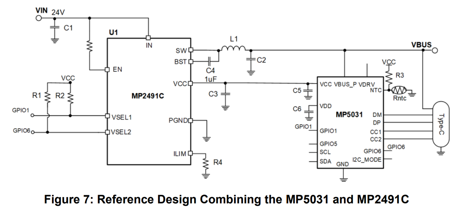
My circuit was based on this diagram:

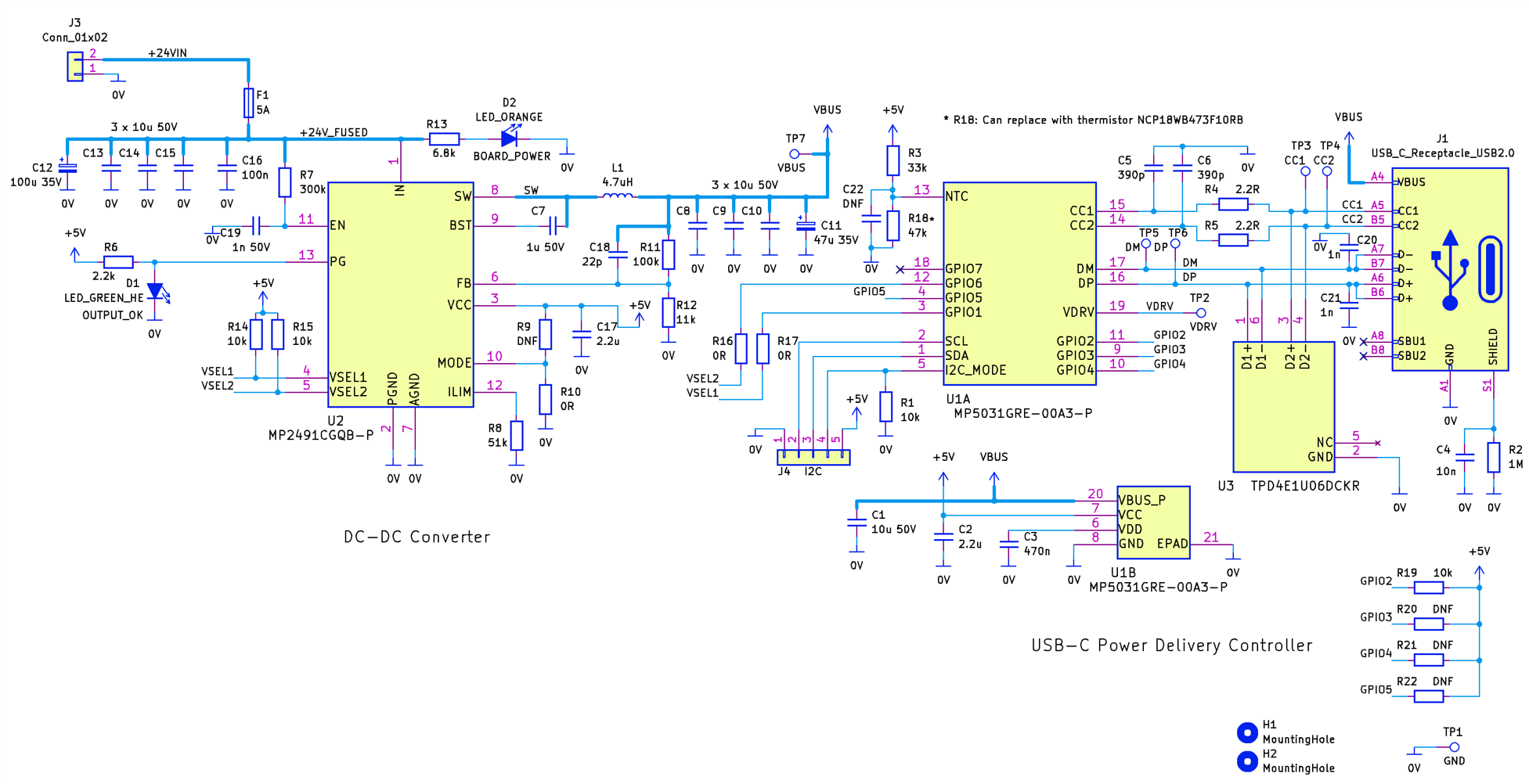
My actual implementation was this (click the diagram to enlarge it):

Programming and Verifying the Chip
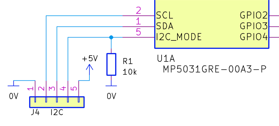
To perform the configuration, I used the connector J4 in the circuit, snippet:

I shorted pins 4 and 5 of the connector (so that I2C_MODE was high which enables the I2C slave), then powered up the board, and then performed the I2C operations using a microcontroller.
The registers inside the chip are all 16-bit wide, and the register addresses are 0x00 to 0x14, with 0x13 missing (it is undocumented, so I didn't read or write that address).
This was the default configuration within the chip (before I wrote my updates):
(note that for each 16-bit register value, the low byte comes first, followed by the high byte, so that (say) "Hex Data F8 02" refers to a register containing the 16-bit value of 0x02F8; this is in accordance with what the datasheet mentions about the order of the bytes over I2C).
Reading chip contents
Reading: Reg: 0x00
         Hex Data: F8 02
Reading: Reg: 0x01
         Hex Data: 64 00
Reading: Reg: 0x02
         Hex Data: 2C 0D
Reading: Reg: 0x03
         Hex Data: B4 00
Reading: Reg: 0x04
         Hex Data: 2C 01
Reading: Reg: 0x05
         Hex Data: 2C 01
Reading: Reg: 0x06
         Hex Data: 2C 01
Reading: Reg: 0x07
         Hex Data: 90 01
Reading: Reg: 0x08
         Hex Data: 2C 01
Reading: Reg: 0x09
         Hex Data: 21 D2
Reading: Reg: 0x0A
         Hex Data: 3C 00
Reading: Reg: 0x0B
         Hex Data: 81 00
Reading: Reg: 0x0C
         Hex Data: 0A 0A
Reading: Reg: 0x0D
         Hex Data: 31 90
Reading: Reg: 0x0E
         Hex Data: F0 98
Reading: Reg: 0x0F
         Hex Data: 3C 3C
Reading: Reg: 0x10
         Hex Data: 00 00
Reading: Reg: 0x11
         Hex Data: 03 00
Reading: Reg: 0x12
         Hex Data: 00 80
Reading: Reg: 0x14
         Hex Data: 00 00
These were the configuration changes I made, there were just three registers I changed:
*** Programming chip ***
#1: Changing register 0x0B from hex 81 00 to 85 00
Writing: Reg: 0x0B
         Hex Data: 85 00
#2: Changing register 0x0D from hex 31 90 to 34 90
Writing: Reg: 0x0D
         Hex Data: 34 90
#3: Changing register 0x0E from hex F0 98 to C8 98
Writing: Reg: 0x0E
         Hex Data: C8 98
*** Programming complete, 3 registers updated ***
After that, I read every register, to ensure each value was expected:
Reading: Reg: 0x00
         Hex Data: F8 02
Register 0x00 contains expected value
Reading: Reg: 0x01
         Hex Data: 64 00
Register 0x01 contains expected value
Reading: Reg: 0x02
         Hex Data: 2C 0D
Register 0x02 contains expected value
Reading: Reg: 0x03
         Hex Data: B4 00
Register 0x03 contains expected value
Reading: Reg: 0x04
         Hex Data: 2C 01
Register 0x04 contains expected value
Reading: Reg: 0x05
         Hex Data: 2C 01
Register 0x05 contains expected value
Reading: Reg: 0x06
         Hex Data: 2C 01
Register 0x06 contains expected value
Reading: Reg: 0x07
         Hex Data: 90 01
Register 0x07 contains expected value
Reading: Reg: 0x08
         Hex Data: 2C 01
Register 0x08 contains expected value
Reading: Reg: 0x09
         Hex Data: 21 D2
Register 0x09 contains expected value
Reading: Reg: 0x0A
         Hex Data: 3C 00
Register 0x0A contains expected value
Reading: Reg: 0x0B
         Hex Data: 85 00
Register 0x0B expected hex 81 00 but chip contains 85 00
Register 0x0B has been programmed with expected update
Reading: Reg: 0x0C
         Hex Data: 0A 0A
Register 0x0C contains expected value
Reading: Reg: 0x0D
         Hex Data: 34 90
Register 0x0D expected hex 31 90 but chip contains 34 90
Register 0x0D has been programmed with expected update
Reading: Reg: 0x0E
         Hex Data: C8 98
Register 0x0E expected hex F0 98 but chip contains C8 98
Register 0x0E has been programmed with expected update
Reading: Reg: 0x0F
         Hex Data: 3C 3C
Register 0x0F contains expected value
Reading: Reg: 0x10
         Hex Data: 00 00
Register 0x10 contains expected value
Reading: Reg: 0x11
         Hex Data: 03 00
Register 0x11 contains expected value
Reading: Reg: 0x12
         Hex Data: 00 80
Register 0x12 contains expected value
Reading: Reg: 0x14
         Hex Data: 00 00
Register 0x14 contains expected value
Chip contents do not match reference blank chip, but match the expected updates.
The chip was successfully programmed previously.
But, after power-cycling the board, this is the result:
Examining chip contents against blank reference chip
Reading: Reg: 0x00
         Hex Data: F8 02
Register 0x00 contains expected value
Reading: Reg: 0x01
         Hex Data: 64 00
Register 0x01 contains expected value
Reading: Reg: 0x02
         Hex Data: 2C 0D
Register 0x02 contains expected value
Reading: Reg: 0x03
         Hex Data: B4 00
Register 0x03 contains expected value
Reading: Reg: 0x04
         Hex Data: 2C 01
Register 0x04 contains expected value
Reading: Reg: 0x05
         Hex Data: 2C 01
Register 0x05 contains expected value
Reading: Reg: 0x06
         Hex Data: 2C 01
Register 0x06 contains expected value
Reading: Reg: 0x07
         Hex Data: 90 01
Register 0x07 contains expected value
Reading: Reg: 0x08
         Hex Data: 2C 01
Register 0x08 contains expected value
Reading: Reg: 0x09
         Hex Data: 21 D2
Register 0x09 contains expected value
Reading: Reg: 0x0A
         Hex Data: 3C 00
Register 0x0A contains expected value
Reading: Reg: 0x0B
         Hex Data: 81 00
Register 0x0B contains expected value
Reading: Reg: 0x0C
         Hex Data: 0A 0A
Register 0x0C contains expected value
Reading: Reg: 0x0D
         Hex Data: 31 90
Register 0x0D contains expected value
Reading: Reg: 0x0E
         Hex Data: F0 98
Register 0x0E contains expected value
Reading: Reg: 0x0F
         Hex Data: 3C 3C
Register 0x0F contains expected value
Reading: Reg: 0x10
         Hex Data: 00 00
Register 0x10 contains expected value
Reading: Reg: 0x11
         Hex Data: 03 00
Register 0x11 contains expected value
Reading: Reg: 0x12
         Hex Data: 00 80
Register 0x12 contains expected value
Reading: Reg: 0x14
         Hex Data: 00 00
Register 0x14 contains expected value
Chip contents match reference blank chip, i.e. chip appears to be unprogrammed
My Configuration Notes
Here is my reasoning for why I modified the register values that I did.
| RegAddr | RegName | Notes | Change |
| 0x00 | PDO_TYPE | Default is OK (all power data objects are enabled). Can read this, to see the software revision. Read 15..0 bits, and bits 15..10 contain the software revision. D0..7 = f8, D8..15 = 02 |
|
| 0x01 | PDO_V1 | Read only. Should return 5V which is 0x064 (only bits 9..0 are relevant). 0x64 x 50mV = 5000mV = 5V | |
| 0x02 | PDO_I1 | Default should be fine, which is 3A (only bits 9..0). 3A/0.01A = 300 which Is 0x12C | |
| 0x03 | PDO_V2 | Default is 9V | |
| 0x04 | PDO_I2 | Default is 3A | |
| 0x05 | PDO_V3 | Default is 15V | |
| 0x06 | PDO_I3 | Default is 3A | |
| 0x07 | PDO_V4 | Default is 20V | |
| 0x08 | PDO_I4 | Default is 3A | |
| 0x09 | PDO_V5 | What is the default? Anyway I left this unchanged. | |
| 0x0A | PDO_I5 | What is the default? I left this unchanged. | |
| 0x0B | CTL1 | Bits 2..0 by default are 0x01 (i.e. 001 binary), but this needs changing! Those three bits need to change to 0x05 (i.e. 101 binary). This sets the chip to be able to select PDO2,3 or 4 by using the PDO2_SEL and PDO3_SEL pins. | Set to hex 85 00 |
| 0x0C | CTL2 | Can write a 1 to the the most significant bit (bit 15) to perform a hard reset. I left this register alone, because I don’t understand some of it. I think the defaults are OK. | |
| 0x0D | CTL3 | Bits 2..0 are by default 001 binary (0x01) but need to be changed to 100 binary (0x04). This makes GPIO1 become VSEL1 (to select 9V). | Set to hex 34 90 |
| 0x0E | CTL4 | Bits 5..3 are by default 010 binary but need to be changed to 001 binary. This makes GPIO6 become VSEL2 (to select 15V). In other words, by setting CTL3 and CTL4, then the voltages that are supported will match the DC-DC converter, and allow 5V, 9V, 15V and 20V, which are PDO1, PDO2, PDO3, and PDO4. |
Set to hex C8 98 |
| 0x0F | PWRSHA | Think this can be left unmodified | |
| 0x10 | STATUS1 | Read-only | |
| 0x11 | STATUS2 | Read-only | |
| 0x12 | ID | Read-only, contains a vendor ID in bits 15..12. Default ID is 1000 binary. | |
| 0x13 | N/A | Undocumented | |
| 0x14 | CLK_ON | No need to modify I think |
Any help appreciated.
Many thanks!
