element14 Community
element14 Community
    Register Log In
  • Site
  • Search
  • Log In Register
  • Community Hub
    Community Hub
    • What's New on element14
    • Feedback and Support
    • Benefits of Membership
    • Personal Blogs
    • Members Area
    • Achievement Levels
  • Learn
    Learn
    • Ask an Expert
    • eBooks
    • element14 presents
    • Learning Center
    • Tech Spotlight
    • STEM Academy
    • Webinars, Training and Events
    • Learning Groups
  • Technologies
    Technologies
    • 3D Printing
    • FPGA
    • Industrial Automation
    • Internet of Things
    • Power & Energy
    • Sensors
    • Technology Groups
  • Challenges & Projects
    Challenges & Projects
    • Design Challenges
    • element14 presents Projects
    • Project14
    • Arduino Projects
    • Raspberry Pi Projects
    • Project Groups
  • Products
    Products
    • Arduino
    • Avnet Boards Community
    • Dev Tools
    • Manufacturers
    • Multicomp Pro
    • Product Groups
    • Raspberry Pi
    • RoadTests & Reviews
  • Store
    Store
    • Visit Your Store
    • Choose another store...
      • Europe
      •  Austria (German)
      •  Belgium (Dutch, French)
      •  Bulgaria (Bulgarian)
      •  Czech Republic (Czech)
      •  Denmark (Danish)
      •  Estonia (Estonian)
      •  Finland (Finnish)
      •  France (French)
      •  Germany (German)
      •  Hungary (Hungarian)
      •  Ireland
      •  Israel
      •  Italy (Italian)
      •  Latvia (Latvian)
      •  
      •  Lithuania (Lithuanian)
      •  Netherlands (Dutch)
      •  Norway (Norwegian)
      •  Poland (Polish)
      •  Portugal (Portuguese)
      •  Romania (Romanian)
      •  Russia (Russian)
      •  Slovakia (Slovak)
      •  Slovenia (Slovenian)
      •  Spain (Spanish)
      •  Sweden (Swedish)
      •  Switzerland(German, French)
      •  Turkey (Turkish)
      •  United Kingdom
      • Asia Pacific
      •  Australia
      •  China
      •  Hong Kong
      •  India
      •  Korea (Korean)
      •  Malaysia
      •  New Zealand
      •  Philippines
      •  Singapore
      •  Taiwan
      •  Thailand (Thai)
      • Americas
      •  Brazil (Portuguese)
      •  Canada
      •  Mexico (Spanish)
      •  United States
      Can't find the country/region you're looking for? Visit our export site or find a local distributor.
  • Translate
  • Profile
  • Settings
Sensors
  • Technologies
  • More
Sensors
Blog Researchers Introduce Metalens Microscope for Medical Applications
  • Blog
  • Forum
  • Documents
  • Quiz
  • Events
  • Polls
  • Members
  • Mentions
  • Sub-Groups
  • Tags
  • More
  • Cancel
  • New
Join Sensors to participate - click to join for free!
  • Share
  • More
  • Cancel
Group Actions
  • Group RSS
  • More
  • Cancel
Engagement
  • Author Author: Catwell
  • Date Created: 10 Jun 2025 7:46 PM Date Created
  • Views 988 views
  • Likes 4 likes
  • Comments 0 comments
  • research
  • on_campus
  • cabeatwell
  • university
  • medical
  • sensor
  • innovation
Related
Recommended

Researchers Introduce Metalens Microscope for Medical Applications

Catwell
Catwell
10 Jun 2025

image

The metalens-based microscope can address off-axis aberrations and achieve high-resolution wide-field imaging. (Image Credit: Tao Li and Jiacheng Sun (Nanjing University))

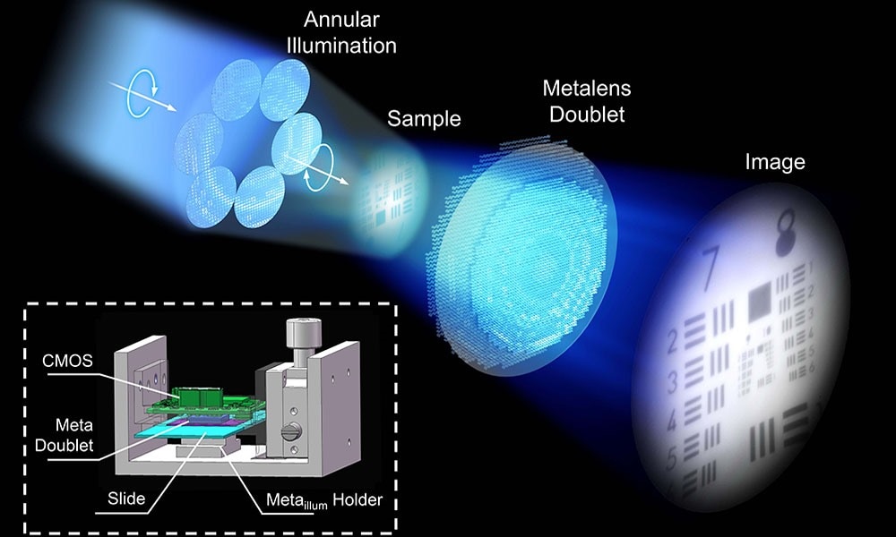
Optical technology could soon change thanks to the introduction of metalenses, which uses nanoscale structures to manipulate light at the subwavelength level. Their lightweight, compact, and ultra-thin design makes them ideal for modern electronics and portable imaging systems. However, metalenses haven't performed as well as traditional microscopes due to the trade-off between field of view (FOV) and resolutions, as well as off-axis aberrations. That could soon change. Researchers at Nanjing University in China developed a wide field of view metalens-based microscope capable of capturing high-resolution images for medical applications. The team believes medical professionals could use it outside laboratory settings without relying on bulky equipment.

To address the limitation, the team deployed a doublet metalense design, which consists of two metalenses placed on each side of a silica substrate combined with annular illumination. Both the metalenses are made of silicon nitride nano-fins, produced as high-aspect-ratio squares with precise dimensions and arranged at carefully calculated intervals. This configuration corrects common distortions and enhances resolution to optimize image performance.

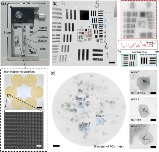
"Our metalens microscope, featuring a FOV of up to 150 μm and a half-pitch-resolution of 310 nm, far exceeds the highest resolution ever reported in meta-microscopy," says corresponding author Dr. Tao Li.

image
The metalense microscope and its application in bio diagnostics. (Image Credit: SPIE Digital Library)

The team's 4 cm x 4 cm x 5 cm portable prototype can image tiny cellular features across a 150-micrometer field with a 310 nanometers resolution. It also achieved 1 mm FOV with a half-pitch resolution of 620 nm. With that capability, the team used the system to image changes in cervical cancer cells that are normally observed under larger laboratory microscopes. They imaged different stages of cancer development within the same FOV, revealing nuclear enlargement, deformation, and division. Medical professionals can improve diagnostic capabilities as it provides them with comprehensive images of tissue samples.

"Our experimental results demonstrate high-quality microscopic bioimages that are comparable to those obtained from traditional microscopes within a compact prototype, highlighting its potential applications in portable and convenient settings," says Li.

This technology could be practical for applications requiring portability and high-performance imaging in mobile monitoring, field research, and low-resource medical settings. It can also be integrated into microelectronic devices for emerging technologies, such as biomedical automation or state-of-the-art systems. The team's breakthrough, which combines performance with portability, leads to high-performance metadevices across optical applications.

Have a story tip? Message me at: http://twitter.com/Cabe_Atwell

  • Sign in to reply
element14 Community

element14 is the first online community specifically for engineers. Connect with your peers and get expert answers to your questions.

  • Members
  • Learn
  • Technologies
  • Challenges & Projects
  • Products
  • Store
  • About Us
  • Feedback & Support
  • FAQs
  • Terms of Use
  • Privacy Policy
  • Legal and Copyright Notices
  • Sitemap
  • Cookies

An Avnet Company © 2025 Premier Farnell Limited. All Rights Reserved.

Premier Farnell Ltd, registered in England and Wales (no 00876412), registered office: Farnell House, Forge Lane, Leeds LS12 2NE.

ICP 备案号 10220084.

Follow element14

  • X
  • Facebook
  • linkedin
  • YouTube