element14 Community
element14 Community
    Register Log In
  • Site
  • Search
  • Log In Register
  • Community Hub
    Community Hub
    • What's New on element14
    • Feedback and Support
    • Benefits of Membership
    • Personal Blogs
    • Members Area
    • Achievement Levels
  • Learn
    Learn
    • Ask an Expert
    • eBooks
    • element14 presents
    • Learning Center
    • Tech Spotlight
    • STEM Academy
    • Webinars, Training and Events
    • Learning Groups
  • Technologies
    Technologies
    • 3D Printing
    • FPGA
    • Industrial Automation
    • Internet of Things
    • Power & Energy
    • Sensors
    • Technology Groups
  • Challenges & Projects
    Challenges & Projects
    • Design Challenges
    • element14 presents Projects
    • Project14
    • Arduino Projects
    • Raspberry Pi Projects
    • Project Groups
  • Products
    Products
    • Arduino
    • Avnet & Tria Boards Community
    • Dev Tools
    • Manufacturers
    • Multicomp Pro
    • Product Groups
    • Raspberry Pi
    • RoadTests & Reviews
  • About Us
  • Store
    Store
    • Visit Your Store
    • Choose another store...
      • Europe
      •  Austria (German)
      •  Belgium (Dutch, French)
      •  Bulgaria (Bulgarian)
      •  Czech Republic (Czech)
      •  Denmark (Danish)
      •  Estonia (Estonian)
      •  Finland (Finnish)
      •  France (French)
      •  Germany (German)
      •  Hungary (Hungarian)
      •  Ireland
      •  Israel
      •  Italy (Italian)
      •  Latvia (Latvian)
      •  
      •  Lithuania (Lithuanian)
      •  Netherlands (Dutch)
      •  Norway (Norwegian)
      •  Poland (Polish)
      •  Portugal (Portuguese)
      •  Romania (Romanian)
      •  Russia (Russian)
      •  Slovakia (Slovak)
      •  Slovenia (Slovenian)
      •  Spain (Spanish)
      •  Sweden (Swedish)
      •  Switzerland(German, French)
      •  Turkey (Turkish)
      •  United Kingdom
      • Asia Pacific
      •  Australia
      •  China
      •  Hong Kong
      •  India
      • Japan
      •  Korea (Korean)
      •  Malaysia
      •  New Zealand
      •  Philippines
      •  Singapore
      •  Taiwan
      •  Thailand (Thai)
      • Vietnam
      • Americas
      •  Brazil (Portuguese)
      •  Canada
      •  Mexico (Spanish)
      •  United States
      Can't find the country/region you're looking for? Visit our export site or find a local distributor.
  • Translate
  • Profile
  • Settings
Sensors
  • Technologies
  • More
Sensors
Blog Solid-State Quantum Microscope Controls the Atomic Qubits’ Wave Functions in Silicon
  • Blog
  • Forum
  • Documents
  • Quiz
  • Events
  • Polls
  • Members
  • Mentions
  • Sub-Groups
  • Tags
  • More
  • Cancel
  • New
Join Sensors to participate - click to join for free!
  • Share
  • More
  • Cancel
Group Actions
  • Group RSS
  • More
  • Cancel
Engagement
  • Author Author: Catwell
  • Date Created: 24 Jul 2023 6:44 PM Date Created
  • Views 600 views
  • Likes 4 likes
  • Comments 0 comments
  • quantum
  • sensors
  • scope
  • on_campus
  • cabeatwell
  • microscope
  • university
  • innovation
Related
Recommended

Solid-State Quantum Microscope Controls the Atomic Qubits’ Wave Functions in Silicon

Catwell
Catwell
24 Jul 2023

image

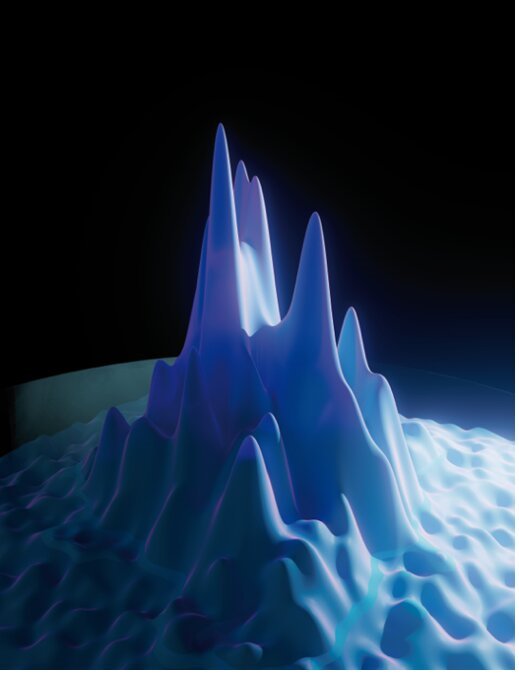
Image showing the wave function of a phosphorous qubit in silicon. (Image Credit: Voisin et al.)

Engineers and physicists have worked on varying technologies like quantum microscopes to leverage quantum mechanical effects. Generally, these microscopes help scientists observe the particles of quantum particles and quantum states in depth. Silicon Quantum Computing (SQC)/UNSW Sydney and the University of Melbourne researchers used ion implantation and atomic precision lithography to develop a solid-state quantum microscope. They believe their microscope can be used for manipulating and investigating the wave function of atomic qubits in silicon.

Researchers at the SQC/UNSW lab manufactured qubit devices and developed scanning tunneling microscopes to image qubit wave functions by using individual phosphorus atoms embedded in silicon. In this latest study, they combined both those research projects into one platform, creating a quantum microscope capable of mapping and controlling atomic qubits with local electrodes in one device.

Their creation was achieved by combining atomic precision lithography to introduce dopant atoms and traditional ion implantation techniques that produce electrodes for the device. "The qubits are defined using the atomic precision manufacturing technique by incorporating a few phosphorus atoms in small patches of desorbed hydrogen at the silicon surface, close to the source electrode," the team says. "Contrary to typical STM experiments performed on conductive substrates, here our microscope operates on insulating silicon, and we had to design a light-assisted protocol to first stabilize the STM tip before being able to map out the qubit wave functions."

The microscope's STM tip works as a moveable electrode, making it more advantageous since it can measure arrays. This method also simplifies the collection of large qubit array measurements without relying on sensors."The ability to map out the qubit wave functions directly during device operation gives us invaluable and predictive insights on how to optimize the device design as we scale, such as distance and orientation between the qubits," the team said. "As a consequence, with regard to the manufacturing of complete circuits using the atomic qubits we engineer at our SQC/UNSW lab, our quantum microscope will help speed up manufacturing cycles for better device performance."

The team believes this study could pave the way to innovative discoveries in the STM and quantum microscopy fields since it's a new quantum microscope fabrication technique. This approach could also apply to solid-state system microscopes, including molecules and magnetic atoms.

The researchers are currently performing microwave coherent operations on the qubits in the microscope to reach beyond the local electrostatic control as described in the paper. Such an achievement requires finite magnetic fields, using new equipment, and sub-100mK temperatures. "The second application we are exploring is to create and probe new correlated states of matter that are challenging to simulate with classical computation techniques or achieve with other experimental platforms such as cold atoms," the team says. "We will fabricate large arrays of qubits strongly coupled to each other in a regime where topological and superconducting states are expected to emerge. This is a very exciting area where our combination of precision manufacturing and ability to see wave functions directly will open new horizons in our atomic understanding of the world."

Have a story tip? Message me at: http://twitter.com/Cabe_Atwell

  • Sign in to reply
element14 Community

element14 is the first online community specifically for engineers. Connect with your peers and get expert answers to your questions.

  • Members
  • Learn
  • Technologies
  • Challenges & Projects
  • Products
  • Store
  • About Us
  • Feedback & Support
  • FAQs
  • Terms of Use
  • Privacy Policy
  • Legal and Copyright Notices
  • Sitemap
  • Cookies

An Avnet Company © 2025 Premier Farnell Limited. All Rights Reserved.

Premier Farnell Ltd, registered in England and Wales (no 00876412), registered office: Farnell House, Forge Lane, Leeds LS12 2NE.

ICP 备案号 10220084.

Follow element14

  • X
  • Facebook
  • linkedin
  • YouTube