element14 Community
element14 Community
    Register Log In
  • Site
  • Search
  • Log In Register
  • Community Hub
    Community Hub
    • What's New on element14
    • Feedback and Support
    • Benefits of Membership
    • Personal Blogs
    • Members Area
    • Achievement Levels
  • Learn
    Learn
    • Ask an Expert
    • eBooks
    • element14 presents
    • Learning Center
    • Tech Spotlight
    • STEM Academy
    • Webinars, Training and Events
    • Learning Groups
  • Technologies
    Technologies
    • 3D Printing
    • FPGA
    • Industrial Automation
    • Internet of Things
    • Power & Energy
    • Sensors
    • Technology Groups
  • Challenges & Projects
    Challenges & Projects
    • Design Challenges
    • element14 presents Projects
    • Project14
    • Arduino Projects
    • Raspberry Pi Projects
    • Project Groups
  • Products
    Products
    • Arduino
    • Avnet Boards Community
    • Dev Tools
    • Manufacturers
    • Multicomp Pro
    • Product Groups
    • Raspberry Pi
    • RoadTests & Reviews
  • Store
    Store
    • Visit Your Store
    • Choose another store...
      • Europe
      •  Austria (German)
      •  Belgium (Dutch, French)
      •  Bulgaria (Bulgarian)
      •  Czech Republic (Czech)
      •  Denmark (Danish)
      •  Estonia (Estonian)
      •  Finland (Finnish)
      •  France (French)
      •  Germany (German)
      •  Hungary (Hungarian)
      •  Ireland
      •  Israel
      •  Italy (Italian)
      •  Latvia (Latvian)
      •  
      •  Lithuania (Lithuanian)
      •  Netherlands (Dutch)
      •  Norway (Norwegian)
      •  Poland (Polish)
      •  Portugal (Portuguese)
      •  Romania (Romanian)
      •  Russia (Russian)
      •  Slovakia (Slovak)
      •  Slovenia (Slovenian)
      •  Spain (Spanish)
      •  Sweden (Swedish)
      •  Switzerland(German, French)
      •  Turkey (Turkish)
      •  United Kingdom
      • Asia Pacific
      •  Australia
      •  China
      •  Hong Kong
      •  India
      •  Korea (Korean)
      •  Malaysia
      •  New Zealand
      •  Philippines
      •  Singapore
      •  Taiwan
      •  Thailand (Thai)
      • Americas
      •  Brazil (Portuguese)
      •  Canada
      •  Mexico (Spanish)
      •  United States
      Can't find the country/region you're looking for? Visit our export site or find a local distributor.
  • Translate
  • Profile
  • Settings
Sensors
  • Technologies
  • More
Sensors
Blog Today I successfully soldered sensor in WLP4 (4 bumps at 0.84 × 0.84mm area)
  • Blog
  • Forum
  • Documents
  • Quiz
  • Events
  • Polls
  • Members
  • Mentions
  • Sub-Groups
  • Tags
  • More
  • Cancel
  • New
Join Sensors to participate - click to join for free!
  • Share
  • More
  • Cancel
Group Actions
  • Group RSS
  • More
  • Cancel
Engagement
  • Author Author: misaz
  • Date Created: 25 Jun 2022 10:10 PM Date Created
  • Views 3003 views
  • Likes 17 likes
  • Comments 3 comments
  • temperature
  • max31875
  • soldering
  • sensor
Related
Recommended

Today I successfully soldered sensor in WLP4 (4 bumps at 0.84 × 0.84mm area)

misaz
misaz
25 Jun 2022

Hello everyone. Today I completed something small but great at once. I first time successfully soldered extremely small sensor - Maxim Integrated MAX31875 I2C temperature sensor. This is sensor is provided as part of MAXESSENTIAL01 Sample Kit which you can receive with corporate or scholar email as a free sample totally for free from Maxim. I did not consider using this sensor in project because I realistically thought that it is impossible to solder in hand and all my projects are soldered in hand. But for fun I designed small breakout PCB, order it at OSHPark for 0.55 USD and tried to solder it.

This sensor has only 4 pins (2 power wires GND and VCC and 2 I2C wires SDA and SCL). It is packed in WLP4 which is kind of package with balls at the bottom. WLP stands for Wafer Level Package and as you guess, chips on wafer are small, so this package is also very small. Package size is only 0.837mm × 0.837mm which is less than milimeter.

image

And really, chip is extremely small. Reading package marking is totally impossible even when using magnifying glass. All following photos are taken by iPhone magnifier tool at maximum possible zoom.
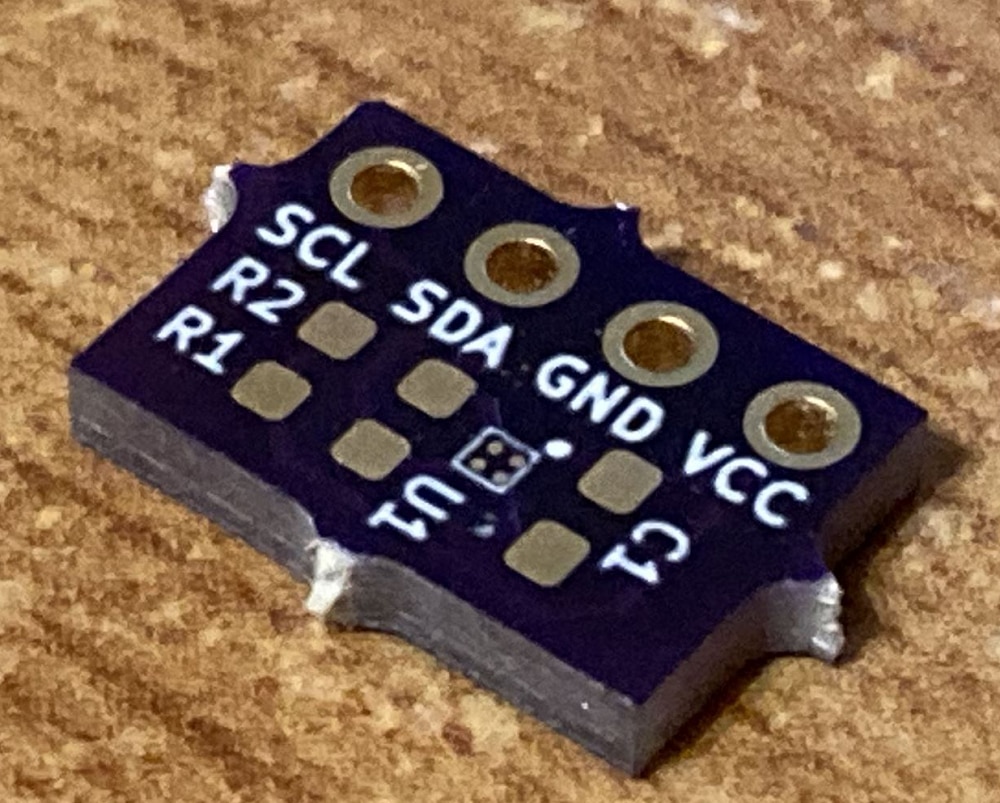
Breakout

This is breakout board to which I attempted to solder sensor:

image

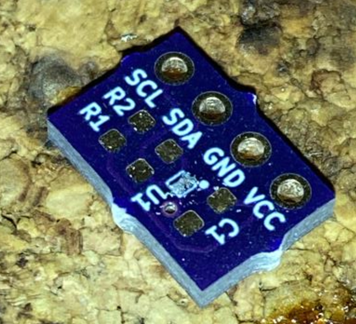
Now you see it extremely zoomed. For reference I recommend taking one 0603 resistor or capacitor to the hand and compare. At the middle you can see highlighted place for MAX31875. As you can see whole temperature sensor is as large as (only) one pad of 0603 footprint! It is smaller than it’s own decoupling capacitor.

Applying Solder Paste

As a next step I applied solder paste. I had no stencil, so I attempted to cover chip area by thin layer of solder paste. Area is very hard to see by eye, so I had to use iPhone magnifier at maximum zoom to check paste application and attempt to clean paste from outside of sensor footprint and reduce thickness of layer. At end it looked as follows:

image

Then I placed a chip to the area. But…

Where is the pin 1 marker?

Find marker of pin number 1 is usually easy, but on chip with sizes less than millimetre it definitely is not. According to documentation pin marking should be in the corner and four letter marking should be at center. But even at maximum zoom of my iPhone camera (aka hobby grade microscope) I see only following glyphs:

image

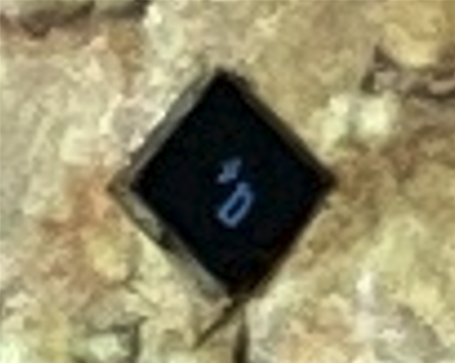
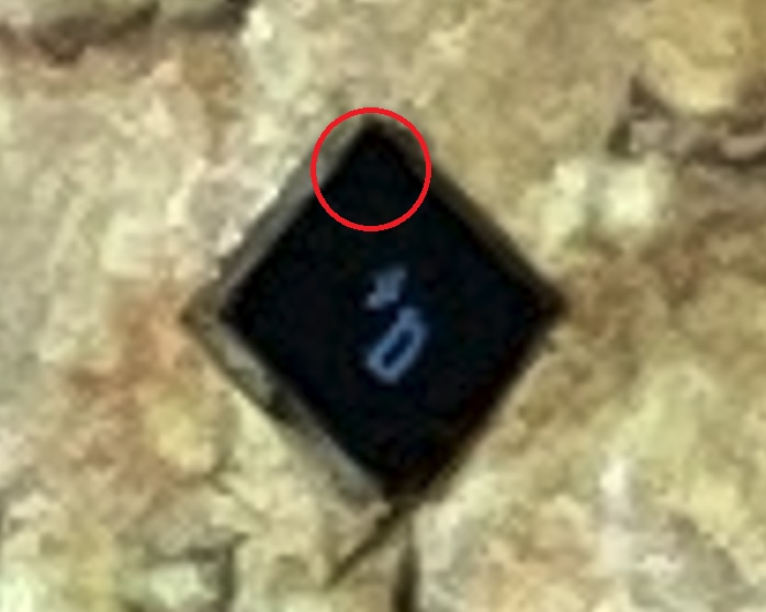
As you can see there is no glyph in the corner. But there is something which looks like Q od D letter and some mark at next to this letter. I had no idea if this is pin 1 marker or pin 1 marker is at the corner, and it is too small for capturing with this camera. But I guessed that symbol near letter is pin 1 marker and assumed that pin 1 is at nearest corner:

image

I placed chip on the board, but unluckily I rotated it when manipulating, so I had to rotate it by 90 deg on the board. Because of small layer of solder paste applied before it was possible to rotate it, but definitely I must say that is not easy to rotate this kind of chips by 90 deg.

After placement I started hot air gun and start heating the board and the sensor. Of course, when doing this I violated absolute maximum rating about temperature and possibly I affected reliability and accuracy of sensor. When soldering at some moment solder paste became bright which I noticed by eye. I also noticed that sensor fit and changed a location a little. At this moment I stopped heating it and wait until temperature of board decrease. Then I tested ESD diodes on pins by multimeter. Diodes between GND and VCC and GND and SDA looked working. I also tested short circuits, but I was unable to sense any connectivity between SCL pin and other wires. I also noticed that after soldering sensor is askew and most probably SCL pin is flaying, and it is not connected to the board Frowning2.

For resolving this issue, I started hot air gun again, heated the sensor again and I tried to push corner containing SCL pin to the board. Of course, my hands are not as precise as required so I moved the senor more than I want and had to reposition it again, but after few attempts it looked good, so I stopped heating and try procedure with ESD diodes test again. Luckily, I sensed ESD diodes on all pins including SCL and I did not measured any short circuit between pins.

I2C Scan

Before I soldered remaining components (decoupling capacitor C1 and I2C pullups R1 and R2) I connected pull-ups on breadboard and touched wires from Raspberry Pi to the board. I started i2cdetect and I successfully detect MAX31875 on the bus! It works!!!!

After this success I soldered remaining components and pinhead, connected sensor to Cypress PSoC 62 board which is not utilized by any project at this time, wrote simple library and simple program for printing temperature measured by this sensor:

image

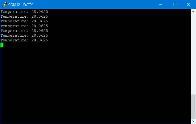
Temperature looks correct, but as I have said above. I don’t know if my double-attempt soldering with violating absolute maximum ratings duration affected sensor accuracy. Later I improved my library and tested advanced features like over-temperature detection and hysteresis. All features of this simple chip works well.

  • Sign in to reply

Top Comments

  • misaz
    misaz over 3 years ago +1
    If someone is interested in trying it on your own, then you can download Kicad project, schematics, gerbers or just order the PCB for 0.55 USD at OSHpark: https://oshpark.com/shared_projects/VH8TeApd …
  • dougw
    dougw over 3 years ago

    Kudos .... Impressive and brave. I don't even like soldering 0603 parts. Even holding a card that small is a problem. I have tried "guess & test" soldering with  hot air a few times, every time it is an adventure with multiple risks - and if there are components nearby, they can get blown away.

    • Cancel
    • Vote Up 0 Vote Down
    • Sign in to reply
    • More
    • Cancel
  • misaz
    misaz over 3 years ago

    If someone is interested in trying it on your own, then you can download Kicad project, schematics, gerbers or just order the PCB for 0.55 USD at OSHpark: https://oshpark.com/shared_projects/VH8TeApd

    There are many libraries for this sensor avalaible online, I published my own library which I have used yesterday to Github: https://github.com/misaz/MAX31875-Library

    According to Summer of Sensors description there would be option to test MAX31875 sensor which I have soldered on EVKIT, you you will get opprotunity to test it without any soldering needed.

    • Cancel
    • Vote Up +1 Vote Down
    • Sign in to reply
    • More
    • Cancel
  • genebren
    genebren over 3 years ago

    Nicely done!  Chips are getting smaller and smaller so our skills need to improve.  I have been thinking about trying some hot air soldering to handle those parts that I can not get in SMD packages with actual pins.

    Good to see that it can be done.

    • Cancel
    • Vote Up 0 Vote Down
    • Sign in to reply
    • More
    • Cancel
element14 Community

element14 is the first online community specifically for engineers. Connect with your peers and get expert answers to your questions.

  • Members
  • Learn
  • Technologies
  • Challenges & Projects
  • Products
  • Store
  • About Us
  • Feedback & Support
  • FAQs
  • Terms of Use
  • Privacy Policy
  • Legal and Copyright Notices
  • Sitemap
  • Cookies

An Avnet Company © 2025 Premier Farnell Limited. All Rights Reserved.

Premier Farnell Ltd, registered in England and Wales (no 00876412), registered office: Farnell House, Forge Lane, Leeds LS12 2NE.

ICP 备案号 10220084.

Follow element14

  • X
  • Facebook
  • linkedin
  • YouTube