


Introduction
This project has been in the back of my mind for ages, and a recent conversation on RF switches with BigG reminded me I really ought to work on it!

The aim of this project is to build a device that can act as a switch for radio frequency (RF) signals. There are various use-cases: it could be useful for antenna switching, or for choosing different filters. Two of the devices could be connected back-to-back with inline attenuators. Quick comparisons could be made through different circuits. The example diagram below shows two sets of multi-throw switches being used to build a switched filter bank.
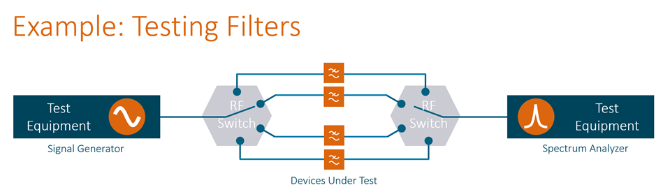
In my case, I was interested in having a way to electronically switch connections for test equipment. It's a real pain having to swap out connections for any of the above scenarios. I'm never quite sure if I've assembled and tightened the connections exactly as before, or if I'm damaging the connectors by too many repeated cycles.
The requirement in the link earlier concerns a requirement for switching RF connections too; BigG wished to experiment with location technologies with Bluetooth Low Energy (BLE) radio signals that need to be routed to/from different antenna connections. While this project is not designed for that use-case, it could, with a slight change in components, be used for that (the adaption would involve swapping out some integrated circuits for different pin-compatible ones, and removing part of the digital circuitry). In summary, then, this project implements a fairly general-purpose building block for RF switching needs at low power.
After completion, this project was used to build a DIY VNA Electronic Calibration Tool with in-built Test Fixture
What does it do?
In a nutshell, the project has five coaxial connectors and operates in a single-pole 4-throw (SP4T) fashion using a push-button. The inputs/outputs to the implemented SP4T switch can be an RF signal from DC up to several Gigahertz.

The RF Switch ICsRF Switch ICs that were used will support up to 9 GHz, but this design cannot support that especially with a low-cost PCB. If it can be useful at 2.4 GHz I'll be very happy!
The ICs used can support 24 dBm (250 mW) of power, which is good for lots of experiments!
The project is powered from 4-5V, and in my case, I will use it from three AA batteries. The same push button can be used to turn the unit on/off. There are four LEDs that indicate how the switch is configured.
How does the RF Switching internally work?
I don't know! In the past, RF switching either required extremely expensive relays or used special diodes (PIN diodes). Diodes are still popular due to the low cost, but such circuits may not operate at very low frequencies or DC. Relays are used for higher power, or for specialist instrumentation. Nowadays, RF switch ICs have become popular for a lot of low-power use-cases. Depending on the type, they might be using transistors for switching, or perhaps MEMs technology for mechanically moving contacts inside the integrated circuit!
Circuit Walkthrough: RF Switching
The core of the project is shown in the circuit diagram below. The design uses three single pole double throw (SPDT) RF switch ICs in two stages. From the left, stage 1 is formed from a single IC U1 that switches the signal path from RF connector J5 to either the top or bottom ICs (U2 or U3). U2 and U3 form stage 2. This stage 2 switches to the connectors on the right, J1-J4.
Two control pins are used for the switch selection, for each stage. The two ICs for stage 2 share common control pins.

There are no DC blocking capacitors in the circuit, so those would need to be added either into the circuit, or externally if there is a risk of a DC offset being present on the RF signals to be controlled.
Switch Selection
The circuit below shows how the four poles of the switch are selected. From the left, a push-button is debounced using a charging/discharging capacitor C9, and this is cleaned up into a logic signal using a Schmitt trigger input inverter, U8. The point labeled A at the output of the inverter is used later on, see further below.
The input to the counter looks unusual in that it is fed to the Enable pin of the counter IC U7, but that's because the 74HC4017 can accept a clock at either pin 13 or 14, and by doing it this way, I can invert the clocking so that the count changes when the button is pressed, rather than when the button is released.
The 74HC4017 is a round-robin type of counter (Johnson counter) and it will cycle SEL1 to SEL4 outputs high, one at a time. Pin 10 is used to reset the count; C16 and R21 are an attempt to reset the counter when the supply is initially attached.

The outputs drive LEDs to indicate which pole is selected.

Controlling the RF Switches
In order to activate the switches, 3.3V logic levels are used and two signals need to be changed for each stage, in order to perform the switching. That's easy enough! A 74HC02 integrated circuit contains four OR gates, and they are combined to provide the appropriate logic based on the SEL pins from the counter IC. From the left, the signal levels are reduced using resistor potential dividers, because the counter IC operates permanently from the unregulated input power source, whereas the RF switch control logic operates at the 3.3V levels that are needed.
The RF switch datasheet was consulted to figure out what logic was needed to convert the counter output into signals that would cycle through the four poles.

Regulated Supply (3.3V)
There's not a lot to say about this portion of circuitry, I followed the 3.3V regulator IC datasheet. Pin 3 is an enable input, labelled B in the circuit diagram, and it is used to switch on the regulator and therefore any circuitry running from the 3.3V output supply rail.

Power On/Off Circuitry
The switch-pole selection push-button also serves to power up/down the rest of the circuit, using the Enable pin on the regulator that was marked B.
In the circuit below, from the left, point A comes from the Schmitt trigger that was attached to the button. If point A is high, then D5 rapidly charges capacitor C15, but if point A is low then resistor R19 slowly discharges it. When the button is held down, point A is low and after a relatively long time (just under a second) the output from inverter U10 will go high and clock the counter IC U9. This IC is being under-used; it's just operating as a divide-by-2 circuit, to provide a toggling action on pin 14, which is connected to point B, which goes to the Enable input to the regulator. Thus, holding down the button will cause the power to switch off or on. Short presses will not allow C15 to discharge fully, and therefore the power status will remain unchanged while the short button presses are being used to control the RF switch poles.
The inverter U6 is redundant, you could just wire the *CLR pin of U9 directly to the supply rail. My original circuit was intended to require a reset mechanism and collapse the 74HC4017 function into a single IC, but I gave up on that, and accidentally left U6 in the circuit. These single gate ICs are cheap; in comparison, each of the RF switch ICs being used costs tenfold, and each of the RF connectors is twentyfold, so I wasn't very motivated to correct the inverter! and so I didn't make changes to the PCB design.

Printed Circuit Board
The top side of the circuit board contains very little; it is primarily dedicated to the RF switches and RF signal paths. The only non-RF components are the four LEDs and the push-button and power supply connection. These could be fitted on the other side if desired (e.g. if it is to be fitted in a metal screening can).

The reason for the weird layout is that I wished to keep everything as symmetrical as possible so that all the signal paths are of identical distance. To work out the physical sizing of the RF signal traces, I used the free Saturn PCB tool (see screenshot below). It computed that if there were copper traces of 14 mil width with a 12 mil gap to the top side ground plane, and there was another ground plane on another layer 7.5 mils below, then the impedance would be 50 ohms. The whole point of the calculation is to get the trace inductance, and the capacitance to ground, 'just right' such that a transmission line is formed that behaves like a coax cable for RF. The close-together holes forms fences (a bit like the microwave oven door operates) to reduce the signal from radiating sideways through the board. The outer edge of the board has bare copper for soldering with a good ground connection into a metal enclosure if that is desired.

The board has four layers and was designed to use the JLCPCB.com prototype PCB service (the trace sizing that was used for the PCB will not function the same if a different board is used).
The screenshot below shows how to configure it on the JLCPCB website if you're interested to reproduce this project. In particular, the layer stackup section is important, it won't work if it's different from the screenshot. The board cost is quite high (about $8 per board, in a quantity of 10, along with a single top-side stencil) but the cost is what it is.
(Click image to enlarge for detail)
The underside of the board houses the remainder of the circuitry, there's not a lot to say about it. Except that it will be far easier to solder that side of the board, than the tiny RF switch ICs on the top side.

Of the two layers of the PCB not shown (the Gerber files are attached to this blog post), the closest layer to the top layer contains just the ground plane, and the next layer down is mostly ground plane apart from a half dozen small traces that were needed for the circuitry that is on the underside of the PCB.
Building It
The components in the section below were ordered, and I started building the board by first soldering the RF switch ICs. I used low-temperature solder paste and a stencil and heated the board from the underside. With the low temperature, I had plenty of time to get those ICs aligned. Next, after the board was cool, I soldered on the three decoupling capacitors for the RF switch ICs, and attached wires to test them. The wires were attached to the four control pins (labelled CTLA1, CTLA2, CTLB1, CTLB2 in the circuit diagram) and the 3.3V supply and 0V, as shown in the photo here.
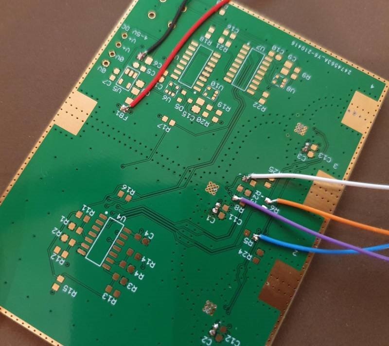
I used a multimeter to check the DC resistance between the RF ports. There's more detail on that in the comments section below. This step was good for checking if the RF switch ICs were correctly soldered or not. It was easy to reflow them again and fix any issues at this stage.
After that, I soldered on all remaining components, with the SMA connectors being the very last step.
There was an issue which needs a few bodge wires; it was found that the power on/off feature was not working, and the rev 1.0 board was permanently powered. To fix it, the following three changes were made (these changes are incorporated in the rev 1.1 board files):
(a) Rotate C16 to isolate one end of it, and solder that to +3V3 at ferrite FB1
(b) Lif pins 14 and 16 of U7, and wire the pins to +3V3 at ferrite FB1 too
(c) Lift pin 13 of U7, and solder a 470k resistor to the lifted pin, and the other end of the resistor is attached to U8 output pin.
The three changes result in the circuit diagram being modified as shown with the red arrows here:

Here is how it looks on the rev 1.0 circuit board:

To solder the SMA connectors, the following procedure was used:
(a) Apply a really tiny dab of solder paste (can use the wire end of a resistor to apply it) as shown in the diagram below onto the two main ground tabs:
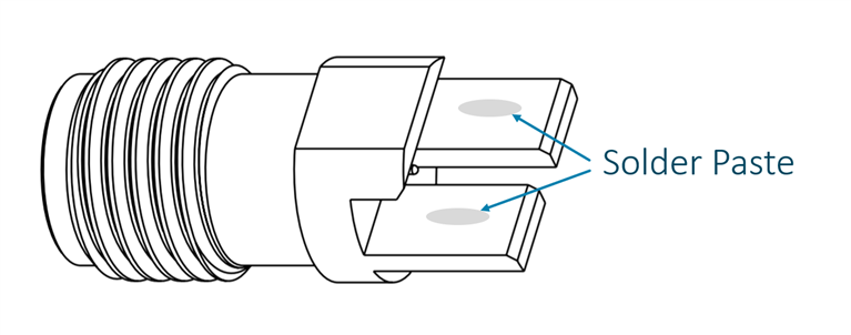
(b) Place the connector where it should go on the PCB, and hold it in place by putting a blob of blu-tack (repositionable temporary putty) on the two tabs. At this stage, the connector will be completely flat against the board, since the two main ground tabs are being used for that alignment.
(c) Now flip the board over gently, and then get a blob of solder on the iron, and apply it to the corner of the SMA connector, without actually touching the metal tip of the iron to the connector. The aim is to only allow the solder blob to touch the connector, so as not to disturb its position, since it is only being held in place with blu-tack on the other side. Aim to tack it in place within a second or so, without softening the blu-tack on the other side! The photo below shows more solder than is required at this stage. It only needs to be lightly tacked, since more solder will be applied to this side later.

(d) Back to the other side of the board, remove the blu-tack and then solder the two main ground tabs properly (don't overheat the connector since you don't want the tacked side to come apart).
(e) Now go back to the tacked side, and apply more solder. I didn't do a great job in the photo above, but perhaps it isn't too critical for a few GHz.
(f) Change soldering iron. Now a 0.2 or 0.4 mm diameter soldering iron tip is needed!
(g) Get a wire-ended resistor, and use a pair of pliers to crush the wire at one end, so it looks like a tiny spatula.
(h) Get a tiny blob of solder paste onto this spatula, and dab it into the centre conductor area. A magnifier is needed to do this ideally.
(i ) Get a tiny blob of solder onto the iron, and then poke it against the end of the centre pin and the circuit board, to try to get the paste to melt and make the join. It's not too difficult, but needs a steady hand not to cause a short circuit to the ground sides. If a short occurs, it is possible to remove it with the 0.2 mm soldering bit, but aim not to need to do that : ) In the phot below, you can see that the left side ground tab has got a bit of solder on it on the inner side, where I was not as careful as I should have been. The right side connector is soldered better.

The final board is shown below. I used a smaller switch, it needed the legs to be bent to fit.

A view from the other side:

A list of all of the main components follows.
Components
First off, the decision needs to be made about which RF switch ICs to use! I selected Renesas F2912Renesas F2912. If higher-speed switches are desired, then they can be replaced with the pin-compatible parts such as pSemi (Peregrine Semiconductor) PE42420. For some RF switch types, the switching control logic can be slightly different. If that is the case, then a different switching logic topology can be invoked by soldering in three resistors in the 'DNF' (do not fit) locations R23-25 on the circuit board, and removing two resistors R6 and R8 (consult the IC datasheet to confirm). The faster switching speed is of less use with the manual push-button control, but the PCB could be patched for control from a microcontroller.
The RF connectors are Amphenol 901-10511-2Amphenol 901-10511-2; a lower-cost option could be to chop the center pin of a more basic connector, to reduce its length because many RF connectors have a thicker center pin that this PCB design isn't intended for. It might work well enough for 1-2 GHz but I don't know for sure.
All of the resistors and most of the capacitors are 0603 sized, however, three 0402 100nF capacitors are used for supply decoupling for the RF switches. Three 0805 sized 2.2uF capacitors are needed.
The ferrite FB1 can be part code HZ0805E601R-10HZ0805E601R-10 but it is not critical and can be swapped with a different 0805 sized one depending on availability.
The four LEDs are 3.2 x 2.8 mm sized and part code SML-Z14DTT86CSML-Z14DTT86C will fit.
Other than the RF switches, the ICs used are: 74HC401774HC4017, 74HC16374HC163, 74HC0274HC02, 3 x 74HC1G1474HC1G14 single gates (love these devices : ) and TPS73433TPS73433.
For the power, I used a 2CR5 battery, Ansmann, 6V, Lithium. It should last for several years with normal use.
Basic Test
As a first test, the tracking generator in the spectrum analyzer (FPC1500) was switched on, the output normalized to remove the effects of the cables, and then the RF switch board was attached and the insertion loss examined.

The screenshot above shows the response between 10 MHz to 3 GHz for J5 being the input port, and J1 being the output port (I tried J1-J4 as output ports, and all had a near-identical response). I think it's not bad, although clearly there is some slight error in the transmission line not being precisely 50 ohms. The insertion loss was under 1.4 dB up to 1 GHz (see marker 1 in the screenshot) although it increased to 3 dB at 3 GHz, and the transmission line error causing an impact too. I think this would be hard to fix without trial-and-error and could change from one PCB manufacturer to the other, for the low-cost 4-layer PCB service. In terms of absolute insertion loss, it is comparable to commercial RF switches (example). The diagram below is from the datasheet of that commercial RF switch.

Summary
RF switches have many uses, this project aims to use RF switch ICs to create a general-purpose RF switching unit for low power signals. The board can accommodate several different RF switch ICs to suit needs, and the control can be push-button operated, or, by not installing some of the components, the board could be operated with a microcontroller.
Thanks for reading!
Top Comments
-

shabaz
-
Cancel
-
Vote Up
+4
Vote Down
-
-
Sign in to reply
-
More
-
Cancel
-

jc2048
in reply to shabaz
-
Cancel
-
Vote Up
+3
Vote Down
-
-
Sign in to reply
-
More
-
Cancel
Comment-

jc2048
in reply to shabaz
-
Cancel
-
Vote Up
+3
Vote Down
-
-
Sign in to reply
-
More
-
Cancel
Children