


The new technique could allow engineers to create new materials with desired properties for applications in data storage, quantum computing, and energy storage. (Image credit: UCI)
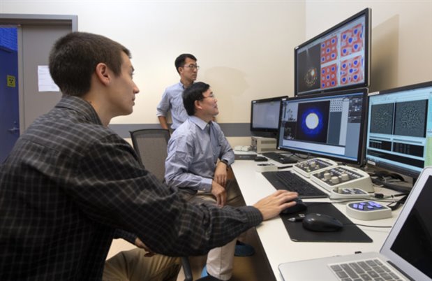
Researchers from the University of California (Irvine) have developed a new scanning transmission electron microscopy technique that allows them to view materials at sub-angstrom levels. The platform is capable of seeing electron distribution between molecules and atoms, giving insights into the roots of ferroelectricity. Ferroelectricity is a unique property of certain materials (in this case crystals) that exhibit spontaneous electric polarization, which can be reversed when an external electric field is present.
According to research team leader professor Xiaoqing Pan, “This method is an advancement in electron microscopy – from detecting atoms to imaging electrons – that could help us engineer new materials with desired properties and functionalities for devices used in data storage, energy conversion, and quantum computing.” The secret to the technique lies in utilizing a new aberration-corrected scanning transmission electron microscope with a fine electron probe the size of half an angstrom, along with a super-fast direct electron detection camera.
The new platform allowed the researchers to garner a 2D raster image of diffraction patterns from an area of interest in a sample material. When collected, the data sets are 4D, which are created utilizing 2D diffraction patterns from each probe site. Pan explains, “With our new microscope, we can routinely form an electron probe as small as 0.6 angstroms, and our high-speed camera with angular resolution can acquire 4D STEM images with 512 x 512 pixels at greater than 300 frames per second. Using this technique, we can see the electron charge distribution between atoms in two different perovskite oxides, non-polar strontium titanate, and ferroelectric bismuth ferrite.”
The researchers state that their new technique provides material scientists and engineers new tools for evaluating frameworks, defects, and interfaces in functional materials and nanodevices, which could lead to breakthroughs in the applications mentioned earlier.
Have a story tip? Message me at: cabe(at)element14(dot)com