element14 Community
element14 Community
    Register Log In
  • Site
  • Search
  • Log In Register
  • About Us
  • Community Hub
    Community Hub
    • What's New on element14
    • Feedback and Support
    • Benefits of Membership
    • Personal Blogs
    • Members Area
    • Achievement Levels
  • Learn
    Learn
    • Ask an Expert
    • eBooks
    • element14 presents
    • Learning Center
    • Tech Spotlight
    • STEM Academy
    • Webinars, Training and Events
    • Learning Groups
  • Technologies
    Technologies
    • 3D Printing
    • FPGA
    • Industrial Automation
    • Internet of Things
    • Power & Energy
    • Sensors
    • Technology Groups
  • Challenges & Projects
    Challenges & Projects
    • Design Challenges
    • element14 presents Projects
    • Project14
    • Arduino Projects
    • Raspberry Pi Projects
    • Project Groups
  • Products
    Products
    • Arduino
    • Avnet Boards Community
    • Dev Tools
    • Manufacturers
    • Multicomp Pro
    • Product Groups
    • Raspberry Pi
    • RoadTests & Reviews
  • Store
    Store
    • Visit Your Store
    • Choose another store...
      • Europe
      •  Austria (German)
      •  Belgium (Dutch, French)
      •  Bulgaria (Bulgarian)
      •  Czech Republic (Czech)
      •  Denmark (Danish)
      •  Estonia (Estonian)
      •  Finland (Finnish)
      •  France (French)
      •  Germany (German)
      •  Hungary (Hungarian)
      •  Ireland
      •  Israel
      •  Italy (Italian)
      •  Latvia (Latvian)
      •  
      •  Lithuania (Lithuanian)
      •  Netherlands (Dutch)
      •  Norway (Norwegian)
      •  Poland (Polish)
      •  Portugal (Portuguese)
      •  Romania (Romanian)
      •  Russia (Russian)
      •  Slovakia (Slovak)
      •  Slovenia (Slovenian)
      •  Spain (Spanish)
      •  Sweden (Swedish)
      •  Switzerland(German, French)
      •  Turkey (Turkish)
      •  United Kingdom
      • Asia Pacific
      •  Australia
      •  China
      •  Hong Kong
      •  India
      •  Korea (Korean)
      •  Malaysia
      •  New Zealand
      •  Philippines
      •  Singapore
      •  Taiwan
      •  Thailand (Thai)
      • Americas
      •  Brazil (Portuguese)
      •  Canada
      •  Mexico (Spanish)
      •  United States
      Can't find the country/region you're looking for? Visit our export site or find a local distributor.
  • Translate
  • Profile
  • Settings
Test & Tools
  • Technologies
  • More
Test & Tools
Blog Programmable Electronic Load - Current Sense Circuit
  • Blog
  • Forum
  • Documents
  • Files
  • Members
  • Mentions
  • Sub-Groups
  • Tags
  • More
  • Cancel
  • New
Join Test & Tools to participate - click to join for free!
  • Share
  • More
  • Cancel
Group Actions
  • Group RSS
  • More
  • Cancel
Engagement
  • Author Author: Jan Cumps
  • Date Created: 16 May 2020 10:29 AM Date Created
  • Views 5718 views
  • Likes 9 likes
  • Comments 32 comments
  • shunt circuit
  • programmable electronic load
  • electronic load
  • programmable
Related
Recommended

Programmable Electronic Load - Current Sense Circuit

Jan Cumps
Jan Cumps
16 May 2020

Detailed review of the current shunt circuit of the Programmable Electronic Load.

image

The circuit and measurements are discussed here.
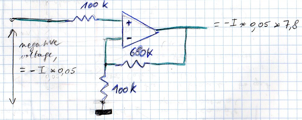
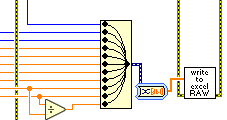
 

Circuit


The current measurement circuit reads the voltage over a 50 mΩ shunt resistor that's in series with the load circuit.


image

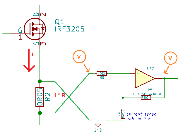
That voltage (always negative, because the resistor is "below" the circuit's analog ground) is amplified by a non-inverting OpAmp circuit, with gain 7.8.


Test Setup


A DMM measures the voltage of the shunt and the output of the OpAmp. Both relative to that analog ground.

image

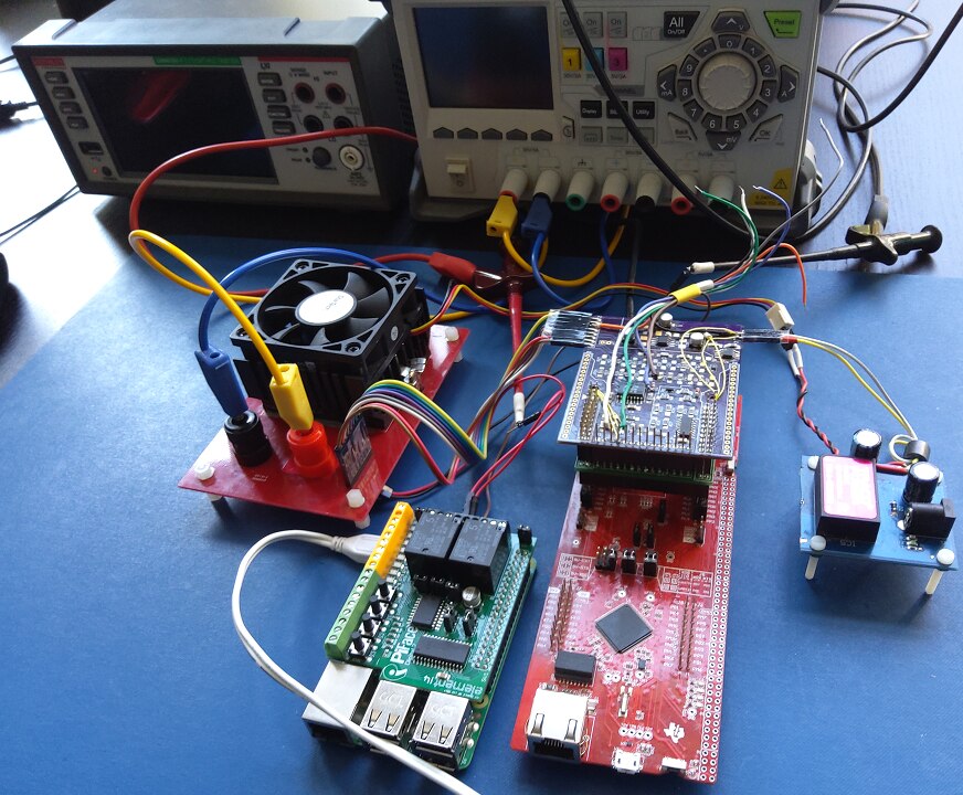
The measurement is automated.

At every iteration, the shunt voltage and the output of the OpAmp are logged.

A relay switches the DMM probe between the two measurement points.

image

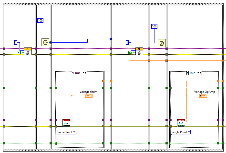
Automated flow detail: switch DMM probe, then take a sample.


I've also added a gain calculation.

imageimage

Gain is calculated as the ratio between output and input. Then logged.


Measurement Results


All data is written to the attached spreadsheet.

The extract below shows 101 measurements.

The DAC that controls the eLoad is set to 0.

A first measurement of current (I take that from the PSU), shunt and OpAmp output voltage are written.

Then, the DAC is 100 times increased, each time with 100. ANd the measurements are repeated.

The attached version (9.xlsx) has more measurements (All eLoad ADCs, and some more stats from the PSU).


image

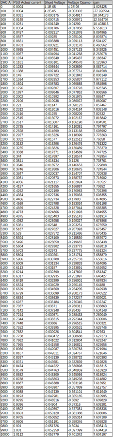
101 samples. PSU = 5 V, DAC initial = 0, steps 100, step 100


Here's a graph of the output vs input. The line represents the gain.

image

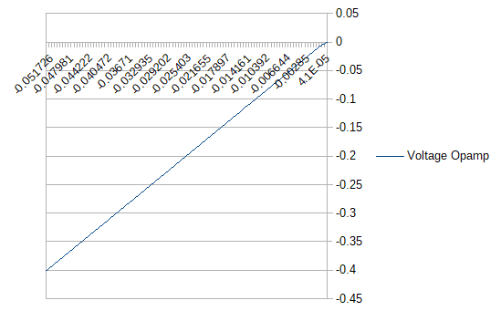
And a graph of the OpAmps gain, with as axis the shunt voltage.

image

Attachments:
eload_dp832a_shunt_circuit_characterisation_9.xlsxeload_dp832a_shunt_circuit_characterisation_9.xlsx
eload_dp832a_shunt_circuit_characterisation_18.zip
eload_dp832a_shunt_circuit_characterisation_19.zip
eload_dp832a_dmm6500_current_2 - workingcopy.zip
  • Sign in to reply

Top Comments

  • Andrew J
    Andrew J over 5 years ago +3
    Interesting. Is this using your compensation approach for the DAC? I presume that the current is being logged by Labview from the Rigol PSU rather than being measured? I think you can do a lot with this…
  • jc2048
    jc2048 over 5 years ago +3
    This is your gain curve but with the vertical axis scaled so we can see what it's doing in more detail. With the exception of a few very odd measurements [settling time? noise?] it has a clearly defined…
  • Jan Cumps
    Jan Cumps over 5 years ago +3
    I've placed the resistor R32 back: As you can see, the board has gone through heavy storms by now. Input: (chart Y axis in µV) Output: (chart Y axis in mV) For those who get stress when seeing a bouncy…
Parents
  • Jan Cumps
    Jan Cumps over 5 years ago

    Advise from Analog Devices on dealing with non-inverting opamp circuit offset.

    https://www.analog.com/media/en/training-seminars/tutorials/MT-037.pdf

    image

    • Cancel
    • Vote Up +3 Vote Down
    • Sign in to reply
    • More
    • Cancel
  • Andrew J
    Andrew J over 5 years ago in reply to Jan Cumps

    Will you give this a go?  I read about the thermal differences between metals somewhere else early this week and thought that it was losing game!  I guess re-calibration of instruments involves things like measuring and tweaking those potentiometers.  Interesting paper.

    • Cancel
    • Vote Up +2 Vote Down
    • Sign in to reply
    • More
    • Cancel
  • Jan Cumps
    Jan Cumps over 5 years ago in reply to Andrew J

    No reason for celebration though. I'm measuring the current sense opamps behaviour over a range of 2000 DAC steps. It ain't nice.


    image


    Way off.

    • Cancel
    • Vote Up +1 Vote Down
    • Sign in to reply
    • More
    • Cancel
  • Andrew J
    Andrew J over 5 years ago in reply to Jan Cumps

    It gets worse as the DAC outputs higher voltages?  The reading is way off as you say - it isn’t subjecting an error to gain is it?

    • Cancel
    • Vote Up +1 Vote Down
    • Sign in to reply
    • More
    • Cancel
  • Jan Cumps
    Jan Cumps over 5 years ago in reply to Andrew J

    It's awful. The shunt voltage is ok, bar a few glitches. Not impacted by the change.

    Measurements attached as 18.zip.

    image

    The output offset, however, has increased:


    image


    I'm going to look first if I can find a trimmer with way less resistance, so that the setting is snugger. And look for a higher R3.


    Then do a few measurements to see if this is better ...

    • Cancel
    • Vote Up +1 Vote Down
    • Sign in to reply
    • More
    • Cancel
  • Jan Cumps
    Jan Cumps over 5 years ago in reply to Andrew J

    With a much lower value trimmer, in this case 10K, the results are way better.

    Measurements attached as 19.zip.

    image

    image

    image


    There is something interesting: the jump that I used to have when the regulation began, is gone.

    Here a capture of today:


    image

    and here one that was done in the past when I was trying to understand that 0 point behaviour of the integrator circuit..


    image

    • Cancel
    • Vote Up +1 Vote Down
    • Sign in to reply
    • More
    • Cancel
  • jc2048
    jc2048 over 5 years ago in reply to Andrew J

    This won't necessarily help Jan much, but it might help you Andrew, or at least give you even more to think about. It's all documented elsewhere, but it's getting so hard to wade through it all I'll repeat it here.


    I used a different op amp to Jan. We were constrained in choice because Peter's initial choice for the circuit had an unusual [wide] footprint, but we wanted to replace it with one with better specs. Jan chose one with FET input transistors (very low current bias, fairly quiet, voltage offset not too good). I would have tried the same, but when I came to buy it couldn't get one so selected a part with bipolar transistors [LT1125] on the input instead (higher bias currents, better offset voltage spec, fairly low noise).


    I got around the poorer bias currents by using a differential amplifier configuration [ie I used the additional resistor placement Jan put on the board] to balance the load on each input better, and by dropping the feedback resistor values considerably [6k8 and 1k]. Reducing the feedback resistors means higher currents in the feedback resistors which reduces the contribution from the amplifier bias currents. I could afford to do that because the shunt is only 50mR. [Peter was concerned about circuit protection, and I'm compromising that, so don't necessarily copy what I've done without thinking of the other aspects of it.]


    I must have been lucky with which way the voltage offset went [I'm struggling to remember now], if there was even much offset at all [datasheet says 100uV max, but you'd be very unlucky to get one at the extreme of the bell curve]. I didn't trim the shunt amplifier, instead I trimmed the integrator op amp to take out the small overall offset round the current-control loop [the integrator amp has an offset too, so adjusting the current sense amplifier to read right won't be enough to get rid of the overall loop offset].


    This was my offset trim. [BTW I wouldn't particularly recommend the Suntan presets. They're cheap, but there's a lot of slop in the lead screw mechanism. Very frustrating if you're trying to adjust something.]


    image


    image


    image


    On a slightly different tack, that picture has reminded me that I put 20M across the integrator capacitor. That's to limit the gain at low frequency. I had a problem that the flicker noise from the op amp input transistors was taking the integrator on a random walk at very low load currents [below a milliamp or two]. The resistors don't entirly get rid of the effect, but do help to reduce it. That might be less of an issue for Jan with his FET input transistors. If you don't do a true PID scheme, with a pure integrator, you might not see it anyway.

    • Cancel
    • Vote Up +2 Vote Down
    • Sign in to reply
    • More
    • Cancel
Comment
  • jc2048
    jc2048 over 5 years ago in reply to Andrew J

    This won't necessarily help Jan much, but it might help you Andrew, or at least give you even more to think about. It's all documented elsewhere, but it's getting so hard to wade through it all I'll repeat it here.


    I used a different op amp to Jan. We were constrained in choice because Peter's initial choice for the circuit had an unusual [wide] footprint, but we wanted to replace it with one with better specs. Jan chose one with FET input transistors (very low current bias, fairly quiet, voltage offset not too good). I would have tried the same, but when I came to buy it couldn't get one so selected a part with bipolar transistors [LT1125] on the input instead (higher bias currents, better offset voltage spec, fairly low noise).


    I got around the poorer bias currents by using a differential amplifier configuration [ie I used the additional resistor placement Jan put on the board] to balance the load on each input better, and by dropping the feedback resistor values considerably [6k8 and 1k]. Reducing the feedback resistors means higher currents in the feedback resistors which reduces the contribution from the amplifier bias currents. I could afford to do that because the shunt is only 50mR. [Peter was concerned about circuit protection, and I'm compromising that, so don't necessarily copy what I've done without thinking of the other aspects of it.]


    I must have been lucky with which way the voltage offset went [I'm struggling to remember now], if there was even much offset at all [datasheet says 100uV max, but you'd be very unlucky to get one at the extreme of the bell curve]. I didn't trim the shunt amplifier, instead I trimmed the integrator op amp to take out the small overall offset round the current-control loop [the integrator amp has an offset too, so adjusting the current sense amplifier to read right won't be enough to get rid of the overall loop offset].


    This was my offset trim. [BTW I wouldn't particularly recommend the Suntan presets. They're cheap, but there's a lot of slop in the lead screw mechanism. Very frustrating if you're trying to adjust something.]


    image


    image


    image


    On a slightly different tack, that picture has reminded me that I put 20M across the integrator capacitor. That's to limit the gain at low frequency. I had a problem that the flicker noise from the op amp input transistors was taking the integrator on a random walk at very low load currents [below a milliamp or two]. The resistors don't entirly get rid of the effect, but do help to reduce it. That might be less of an issue for Jan with his FET input transistors. If you don't do a true PID scheme, with a pure integrator, you might not see it anyway.

    • Cancel
    • Vote Up +2 Vote Down
    • Sign in to reply
    • More
    • Cancel
Children
  • Jan Cumps
    Jan Cumps over 5 years ago in reply to jc2048

    jc2048  wrote:


    ..... I didn't trim the shunt amplifier, instead I trimmed the integrator op amp to take out the small overall offset round the current-control loop [the integrator amp has an offset too, so adjusting the current sense amplifier to read right won't be enough to get rid of the overall loop offset]...


    I compensate both at the moment - the current sense one with the trimpot just added here, the integrator by injecting DAC2 output.

    • Cancel
    • Vote Up +2 Vote Down
    • Sign in to reply
    • More
    • Cancel
  • Andrew J
    Andrew J over 5 years ago in reply to jc2048

    Thanks Jon - there is a lot to read and I struggle to follow all of it across multiple threads.  I think it would help if I was building one of these as I could keep a thread of the story going.  Having said that, in the process of designing my control board and breadboarding elements of it I'm discovering some of the issues and then 'see the light', as it were, on some of these thread discussions and understand what you are doing (for example, looking at using an Opamp to subtract offset voltage for a DAC and then having it click what Jan is/was doing with his tiny add-on board.)


    At the moment, I'm concentrating on just a control board to better understand both DAC and ADC operation but also now, as it seems unavoidable, Op Amps alongside these components.  I did some analysis of a number of Op Amps based on my limited understanding and settled on a OPA192 from TI.  I have written up my reasoning but haven't posted it yet as I'm working on a prototype design to test some of this with different configurations - really, I don't have enough empirical experience to know whether I'm making good/flawed choices so I want to test some of this. But also because it's absolutely fascinating to me.  I'm particularly interested in what Jan is doing here as it may be useful to add something into my prototype rather than try and bodge it in later. When it's all ready, I'll post.


    I suspect that as I go through testing the prototype, more of what you guys have been posting will make sense as elements will click into place.  At least, that's my hope.


    What I want to do with the prototype, in summary:

    • Try different ADCs to see if I can work out a trade-off between specs and functionality.
    • For each: 1 channel buffered with LPF using the ADC to apply gain; 1 channel gained-up by x2, with LPF; 1 channel buffered with no LPF, ADC providing gain; 1 channel unbuffered with the ADC providing gain. So the first three configurations use an OpAmp in front of the ADC input, the last configuration doesn't.
    • Compensation with DAC and ADC - something explored by Jan with an add on board and also with this work here.


    I know your work is all based on the DC load, but a useful question might be: if you guys could go back again is there anything you would have wanted space/pads to try out?

    • Cancel
    • Vote Up +2 Vote Down
    • Sign in to reply
    • More
    • Cancel
  • Jan Cumps
    Jan Cumps over 5 years ago in reply to Andrew J

    Andrew J  wrote:


    ... there is a lot to read and I struggle to follow all of it across multiple threads.  .....

    This is true. It has to do with posting what happens and then think about why it happens. It has been the style throughout the build of the project.

    If you follow real-time, things (could) make sense. But reading through it after the facts, with discussions driving decisions driving discussions, isn't easy.

    Part of that I try to solve in the main posts. They have a little bit of story line in them and I try to clean them out when the design changes.

    The comments show the rough road. Not a good read, but a lot of what was learned during the project happened there.

    • Cancel
    • Vote Up +3 Vote Down
    • Sign in to reply
    • More
    • Cancel
  • Jan Cumps
    Jan Cumps over 5 years ago in reply to Andrew J

    Andrew J  wrote:


    ...

    I know your work is all based on the DC load, but a useful question might be: if you guys could go back again is there anything you would have wanted space/pads to try out?

    On the analog board: more footprints for the OpAmp. There was place on the board to have the current OpAmp footprint supported, but also accommodate the more common, narrower footprint used by a wider range of quad OpAmps.

    This would have been possible with not too much work. But it didn't happen.

    For the rest I haven't regretted the design. You can't predict the future so whatever flex you build in, it's not going to be the right flex for the particular change you want to make.

    So I don't regret that there's no room for compensation, adjustment, improvement components. There's good access to every node of the circuit to hack, and the bottom side has plenty of space for additional components.

    ... as long as you're willing to break out the solder iron.


    On the DAC/ADC board, I regret selecting too small footprint ICs. I did it for a reason: I wanted to train myself on compact small footprint design/build and used that board to do that. But it's difficult to build (also because I made a mistake in one of the footprints and it requires clipping away IC pins image ) and almost impossible to hack/mod.

    • Cancel
    • Vote Up +3 Vote Down
    • Sign in to reply
    • More
    • Cancel
  • Andrew J
    Andrew J over 5 years ago in reply to Jan Cumps

    It's still really interesting which is why I've started on something similar.  I wanted to understand it better for myself so I'm not replicating exactly what you have done - although in fairness, there's only so many ways you can deploy a DAC and ADC! - which has led to some lightbulb moments as I say.  Hopefully more to come.

    • Cancel
    • Vote Up +2 Vote Down
    • Sign in to reply
    • More
    • Cancel
element14 Community

element14 is the first online community specifically for engineers. Connect with your peers and get expert answers to your questions.

  • Members
  • Learn
  • Technologies
  • Challenges & Projects
  • Products
  • Store
  • About Us
  • Feedback & Support
  • FAQs
  • Terms of Use
  • Privacy Policy
  • Legal and Copyright Notices
  • Sitemap
  • Cookies

An Avnet Company © 2025 Premier Farnell Limited. All Rights Reserved.

Premier Farnell Ltd, registered in England and Wales (no 00876412), registered office: Farnell House, Forge Lane, Leeds LS12 2NE.

ICP 备案号 10220084.

Follow element14

  • X
  • Facebook
  • linkedin
  • YouTube