


Ground loops are a mystery to many people. Even seasoned electronic engineers can struggle to understand the concept of ground loops. This is generally because either the engineer is focused on designing the power distribution system or the equipment that plugs into the power distribution system. Ground loops can cause issues in a variety of equipment and systems. These can be audio and video systems, communication systems, and electronic equipment in general. The issues ground loops cause are generally non-destructive and arise in the form of excess noise or distortion.
Before exploring what a ground loop actually is, let's review the meaning of ground in electronics. Ground can have a variety of meanings in electronics, but generally, there are two types of grounds. There is a chassis or "Earth" ground and printed circuit board (PCB) ground. The chassis ground is a safety feature in electronic systems and appliances. It is present in systems such that if a wire's insulation wears down and opens, allowing the wire to short to the chassis, the extra energy and current will flow into the Earth ground. If that was not the case, the chassis would be "live," and if anyone was to touch it, they would get electrocuted. On the other hand, the PCB ground refers to a common point on a circuit board that is at 0V. This ground, in theory can source or sink any amount of current and provides a common return path for all signals' current flow. In reality, no perfect ground exists. Since all conductors have some amount of resistance, a voltage drop will develop when current flows through the conductor. Consequently, depending on the physical location a circuit is referencing for ground, the conductor may not actually be at 0V.
Moving back to ground loops, they happen to occur when two separate devices are connected to ground as well as to each other. The basic idea is shown in the diagram below. Basically, the connection between the two devices will have some signal wire (or wires) and ground connections. In addition, each device is separately plugged into a wall outlet with an Earth ground connection that is common to the electrical distribution system. As a result, a loop is formed, which can act as a loop antenna. By itself, this loop is not so much of an issue. However, in the presence of stray electromagnetic energy, electromagnetic induction causes current to flow in the loop resulting in some amount of voltage drop developing on the ground conductor. This voltage can be time-varying and thus will show up as noise on the signal paths. A moving ground is in no situation a good ground.

Diagram demonstrating how a ground loop can be formed with two devices. (Image credit: Me)
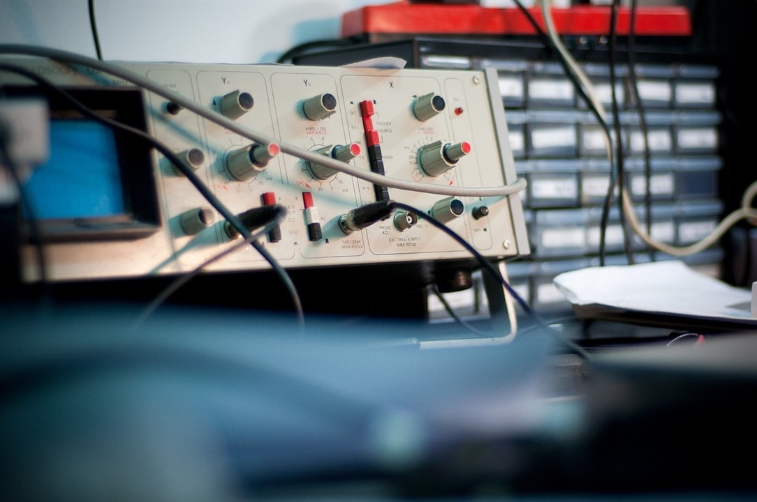
In electronic test equipment, ground loops can occur in oscilloscopes when trying to probe and test electrical circuits. If the circuits under test are being powered by a battery or by a two-prong electrical wire, no loop can form. However, if trying to test a device that is powered through a wall outlet with a three-prong cable, there is the potential for a ground loop to form. This occurs once the ground connection on the probe makes contact with the circuit ground. Referring to the previous diagram, device 1 is the circuit under test, and device 2 is the oscilloscope. They already share a common ground through the Earth connection. Once the probe ground makes a connection with the circuit under test, it completes a ground loop. This loop can introduce noise into the system. Furthermore, the larger the loop, the more noise the loop will pick up. If ground loops are a concern or an issue when testing with an oscilloscope, a few actions can be done to help eliminate the issue. First, the user can try to decrease the size of the loop. This can be done by attempting to power the devices through the same outlets. If that doesn't work a differential probe can be used to help with the issue. For the best possible solution, the device under test can be powered through an isolation transformer. Overall, ground loops are tricky and can present challenges in systems and equipment. A user must always remember that no perfect ground exists and always consider the possibilities of distortion ground loops can present.
Have a story tip? Message me at: http://twitter.com/Cabe_Atwell
