element14 Community
element14 Community
    Register Log In
  • Site
  • Search
  • Log In Register
  • About Us
  • Community Hub
    Community Hub
    • What's New on element14
    • Feedback and Support
    • Benefits of Membership
    • Personal Blogs
    • Members Area
    • Achievement Levels
  • Learn
    Learn
    • Ask an Expert
    • eBooks
    • element14 presents
    • Learning Center
    • Tech Spotlight
    • STEM Academy
    • Webinars, Training and Events
    • Learning Groups
  • Technologies
    Technologies
    • 3D Printing
    • FPGA
    • Industrial Automation
    • Internet of Things
    • Power & Energy
    • Sensors
    • Technology Groups
  • Challenges & Projects
    Challenges & Projects
    • Design Challenges
    • element14 presents Projects
    • Project14
    • Arduino Projects
    • Raspberry Pi Projects
    • Project Groups
  • Products
    Products
    • Arduino
    • Avnet Boards Community
    • Dev Tools
    • Manufacturers
    • Multicomp Pro
    • Product Groups
    • Raspberry Pi
    • RoadTests & Reviews
  • Store
    Store
    • Visit Your Store
    • Choose another store...
      • Europe
      •  Austria (German)
      •  Belgium (Dutch, French)
      •  Bulgaria (Bulgarian)
      •  Czech Republic (Czech)
      •  Denmark (Danish)
      •  Estonia (Estonian)
      •  Finland (Finnish)
      •  France (French)
      •  Germany (German)
      •  Hungary (Hungarian)
      •  Ireland
      •  Israel
      •  Italy (Italian)
      •  Latvia (Latvian)
      •  
      •  Lithuania (Lithuanian)
      •  Netherlands (Dutch)
      •  Norway (Norwegian)
      •  Poland (Polish)
      •  Portugal (Portuguese)
      •  Romania (Romanian)
      •  Russia (Russian)
      •  Slovakia (Slovak)
      •  Slovenia (Slovenian)
      •  Spain (Spanish)
      •  Sweden (Swedish)
      •  Switzerland(German, French)
      •  Turkey (Turkish)
      •  United Kingdom
      • Asia Pacific
      •  Australia
      •  China
      •  Hong Kong
      •  India
      •  Korea (Korean)
      •  Malaysia
      •  New Zealand
      •  Philippines
      •  Singapore
      •  Taiwan
      •  Thailand (Thai)
      • Americas
      •  Brazil (Portuguese)
      •  Canada
      •  Mexico (Spanish)
      •  United States
      Can't find the country/region you're looking for? Visit our export site or find a local distributor.
  • Translate
  • Profile
  • Settings
Test & Tools
  • Technologies
  • More
Test & Tools
Forum Moving pads to back of a PCB in KiCad
  • Blog
  • Forum
  • Documents
  • Files
  • Members
  • Mentions
  • Sub-Groups
  • Tags
  • More
  • Cancel
  • New
Join Test & Tools to participate - click to join for free!
Actions
  • Share
  • More
  • Cancel
Forum Thread Details
  • State Verified Answer
  • Replies 3 replies
  • Subscribers 356 subscribers
  • Views 5662 views
  • Users 0 members are here
  • kicad
  • pcb layout
Related

Moving pads to back of a PCB in KiCad

three-phase
three-phase over 4 years ago

I am having another go at creating a test board for the Hioki BT3554 I roadtested a couple of weeks back.


I have progressed slightly after doubling up the pads and tracks in my schematic and this has now allowed me to add the vias through from the front to the back copper tracks. I am still confused by the copper pad positioning and wonder if someone could assist.


Once I have imported all of the pads and components using the Netlist, I am able to position them all, but everything is initially all on the front copper.


image


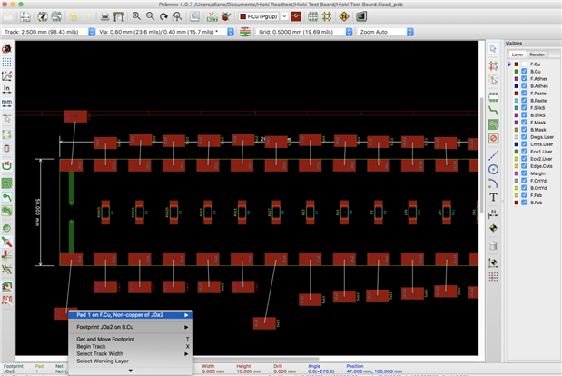
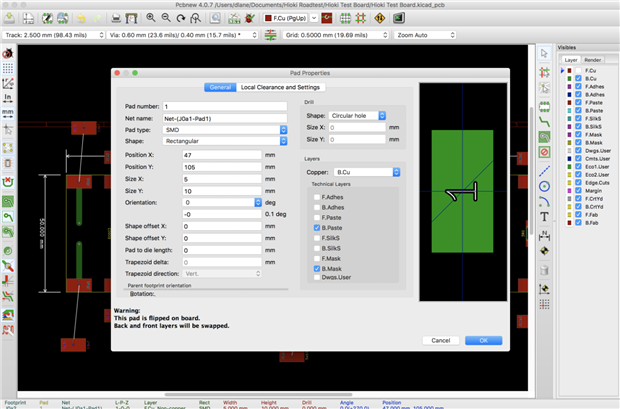
I go into the properties for the relevant pad and the footprint to convert them from front copper to back copper. On the popup menu, the footprint shows as being on the back copper, but the pad does not, and it does not change to the back copper colour.


image


However, in the properties, the pad is marked as being on the back copper, but there is a warning that it is flipped.


image


Can anyone provide any guidance on where I am going wrong? The aim is to have a pads on the front and back copper so that a kelvin clip could be placed over them to make contact with both sides.

  • Sign in to reply
  • Cancel

Top Replies

  • hlipka
    hlipka over 4 years ago +6 verified
    You do not move single pads to the back copper, but the whole component (aka 'footprint'). Do this by using 'f' (for 'flip'). When you want to have back and front copper for a single footprint, you do…
  • hlipka
    0 hlipka over 4 years ago

    You do not move single pads to the back copper, but the whole component (aka 'footprint'). Do this by using 'f' (for 'flip'). When you want to have back and front copper for a single footprint, you do that in the footprint editor, not in PCBNew. In the foot print editor you can have multiple pads for the same pin.

    • Cancel
    • Vote Up +6 Vote Down
    • Sign in to reply
    • Verify Answer
    • Reject Answer
    • Cancel
  • three-phase
    0 three-phase over 4 years ago in reply to hlipka

    Many thanks for your help. I couldn't get multiple pads in the footprint editor, it just gave me an error message, but using the flip function appears to have worked.


    I guess I will send the board away and see what comes back.


    Kind regards.

    • Cancel
    • Vote Up 0 Vote Down
    • Sign in to reply
    • Verify Answer
    • Cancel
  • hlipka
    0 hlipka over 4 years ago in reply to three-phase

    Do you mean you did not get multiple pads at all in the FP editor? Or not on both sides? For the latter, check this discussion: https://www.reddit.com/r/KiCad/comments/bele2z/double_sided_footprint/ (basically a pad has a layer property which you can change between front and back copper).

    • Cancel
    • Vote Up 0 Vote Down
    • Sign in to reply
    • Verify Answer
    • Cancel
element14 Community

element14 is the first online community specifically for engineers. Connect with your peers and get expert answers to your questions.

  • Members
  • Learn
  • Technologies
  • Challenges & Projects
  • Products
  • Store
  • About Us
  • Feedback & Support
  • FAQs
  • Terms of Use
  • Privacy Policy
  • Legal and Copyright Notices
  • Sitemap
  • Cookies

An Avnet Company © 2025 Premier Farnell Limited. All Rights Reserved.

Premier Farnell Ltd, registered in England and Wales (no 00876412), registered office: Farnell House, Forge Lane, Leeds LS12 2NE.

ICP 备案号 10220084.

Follow element14

  • X
  • Facebook
  • linkedin
  • YouTube