element14 Community
element14 Community
    Register Log In
  • Site
  • Search
  • Log In Register
  • Community Hub
    Community Hub
    • What's New on element14
    • Feedback and Support
    • Benefits of Membership
    • Personal Blogs
    • Members Area
    • Achievement Levels
  • Learn
    Learn
    • Ask an Expert
    • eBooks
    • element14 presents
    • Learning Center
    • Tech Spotlight
    • STEM Academy
    • Webinars, Training and Events
    • Learning Groups
  • Technologies
    Technologies
    • 3D Printing
    • FPGA
    • Industrial Automation
    • Internet of Things
    • Power & Energy
    • Sensors
    • Technology Groups
  • Challenges & Projects
    Challenges & Projects
    • Design Challenges
    • element14 presents Projects
    • Project14
    • Arduino Projects
    • Raspberry Pi Projects
    • Project Groups
  • Products
    Products
    • Arduino
    • Avnet Boards Community
    • Dev Tools
    • Manufacturers
    • Multicomp Pro
    • Product Groups
    • Raspberry Pi
    • RoadTests & Reviews
  • About Us
  • Store
    Store
    • Visit Your Store
    • Choose another store...
      • Europe
      •  Austria (German)
      •  Belgium (Dutch, French)
      •  Bulgaria (Bulgarian)
      •  Czech Republic (Czech)
      •  Denmark (Danish)
      •  Estonia (Estonian)
      •  Finland (Finnish)
      •  France (French)
      •  Germany (German)
      •  Hungary (Hungarian)
      •  Ireland
      •  Israel
      •  Italy (Italian)
      •  Latvia (Latvian)
      •  
      •  Lithuania (Lithuanian)
      •  Netherlands (Dutch)
      •  Norway (Norwegian)
      •  Poland (Polish)
      •  Portugal (Portuguese)
      •  Romania (Romanian)
      •  Russia (Russian)
      •  Slovakia (Slovak)
      •  Slovenia (Slovenian)
      •  Spain (Spanish)
      •  Sweden (Swedish)
      •  Switzerland(German, French)
      •  Turkey (Turkish)
      •  United Kingdom
      • Asia Pacific
      •  Australia
      •  China
      •  Hong Kong
      •  India
      •  Korea (Korean)
      •  Malaysia
      •  New Zealand
      •  Philippines
      •  Singapore
      •  Taiwan
      •  Thailand (Thai)
      • Americas
      •  Brazil (Portuguese)
      •  Canada
      •  Mexico (Spanish)
      •  United States
      Can't find the country/region you're looking for? Visit our export site or find a local distributor.
  • Translate
  • Profile
  • Settings
Bluetooth Unleashed Design Challenge
  • Challenges & Projects
  • Design Challenges
  • Bluetooth Unleashed Design Challenge
  • More
  • Cancel
Bluetooth Unleashed Design Challenge
Blog Smart Doorbell System – Part 2 – Creating Parts and Footprints
  • Blog
  • Forum
  • Documents
  • Polls
  • Files
  • Events
  • Mentions
  • Sub-Groups
  • Tags
  • More
  • Cancel
  • New
  • Share
  • More
  • Cancel
Group Actions
  • Group RSS
  • More
  • Cancel
Engagement
  • Author Author: shabaz
  • Date Created: 15 May 2018 2:32 PM Date Created
  • Views 817 views
  • Likes 13 likes
  • Comments 4 comments
  • bluetooth
  • cc2640r2
  • ti launchpad
  • bluetooth le
  • bluetooth_unleashed
  • bt_smart_doorbell
  • design_challenges
  • bluetooth 5.0
  • texas_instruments
  • cc2640r2f
  • texas instruments
  • bluetooth_le
Related
Recommended

Smart Doorbell System – Part 2 – Creating Parts and Footprints

shabaz
shabaz
15 May 2018

For all parts to this project, click here! Smart Doorbell System


Introduction

The Smart Doorbell System is an idea for a home bell-push/chime system with better range and features than expected from existing systems!


It relies on Bluetooth LE for communication; the system is wireless. In order to get there, the design will make use of the Texas Instruments CC2640R2F wireless chip, in both the bell push and the chime modules. This chip contains processing and wireless capabilities all-in-one. To get started with this chip, a CC2640R2 development boardCC2640R2 development board is available.


image


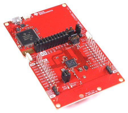
Since this design challenge is a complete project, the steps to get there will require involve producing a design from the requirements, and implementing it in software and hardware. There will be software development and debugging to do, and schematic entry, PCB layout and CAD design. The first part Smart Doorbell System - Part 1 - Getting to know the CC2640R2  examined the development board from TI, called the CC2640R2 LaunchPad (most of TI's microcontroller development boards are called LaunchPads - they all have a similar layout with dual 20-way headers for attaching daughter boards called BoosterPacks).


The LaunchPad contains the CC2640R2F integrated circuit (in a 40-pin VQFN package) along with a programmer/debugger that connects to the PC using USB. It was also explored how Autodesk Fusion could be used to directly create an enclosure based on the PCB information.


PCBs can take a while to manufacture and get delivered, so I wanted to get a move on and at least prepare for it now, so that it can be worked on as the design progresses. This blog post discusses the CC2640R2F part creation in Autodesk EAGLE which is useful for laying out circuits and PCBs.


Some Initial PCB and Component Considerations

Life has been made quite easy with the CC2640R2 LaunchPad, because it comes with a full itemised list of parts on the board (CC2640R2 Launchpad documentation link scroll down to Design Files). Therefore for reduced risk I can chose similar or identical crystals for example. The LaunchPad board has an integrated PCB antenna, but I may choose to use a different antenna (and perhaps different for the bell push module and for the chime module). Since element14 kindly provided a budget, I used some of it to purchase some antennas so I can try them out. Many antennas intended for consumer applications tended to have reverse-polarity SMA connectors to prevent users from attaching high-gain directional antennas, and there are legal requirements in some countries regarding connectors and removable or fixed antenna selection. For the purposes of this prototype, a standard connector will be used, but a commercial design will need to swap it out to suit any current legislation in its intended market.


As part of the antenna matching procedure, space will be left on the PCB for soldering inductors or capacitors to provide for the ideal match between the source and load, so that communication range can be good.


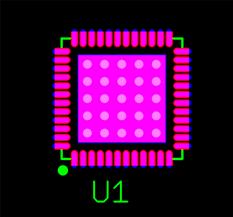
PCB Land Pattern Creation with EAGLE

I’m using a slightly older version of Autodesk EAGLEAutodesk EAGLE, so the procedure may have changed in recent times. Rachael’s ( rachaelp ) excellent EAGLE tutorial can be used as a guide. I used the CC2640R2F datasheet to obtain all the measurements.


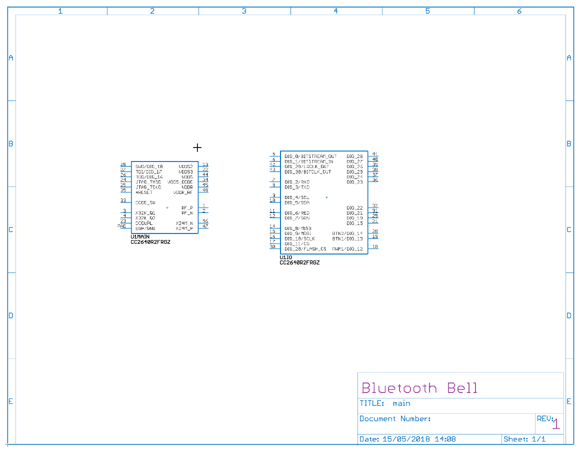
The final part is shown here:

image


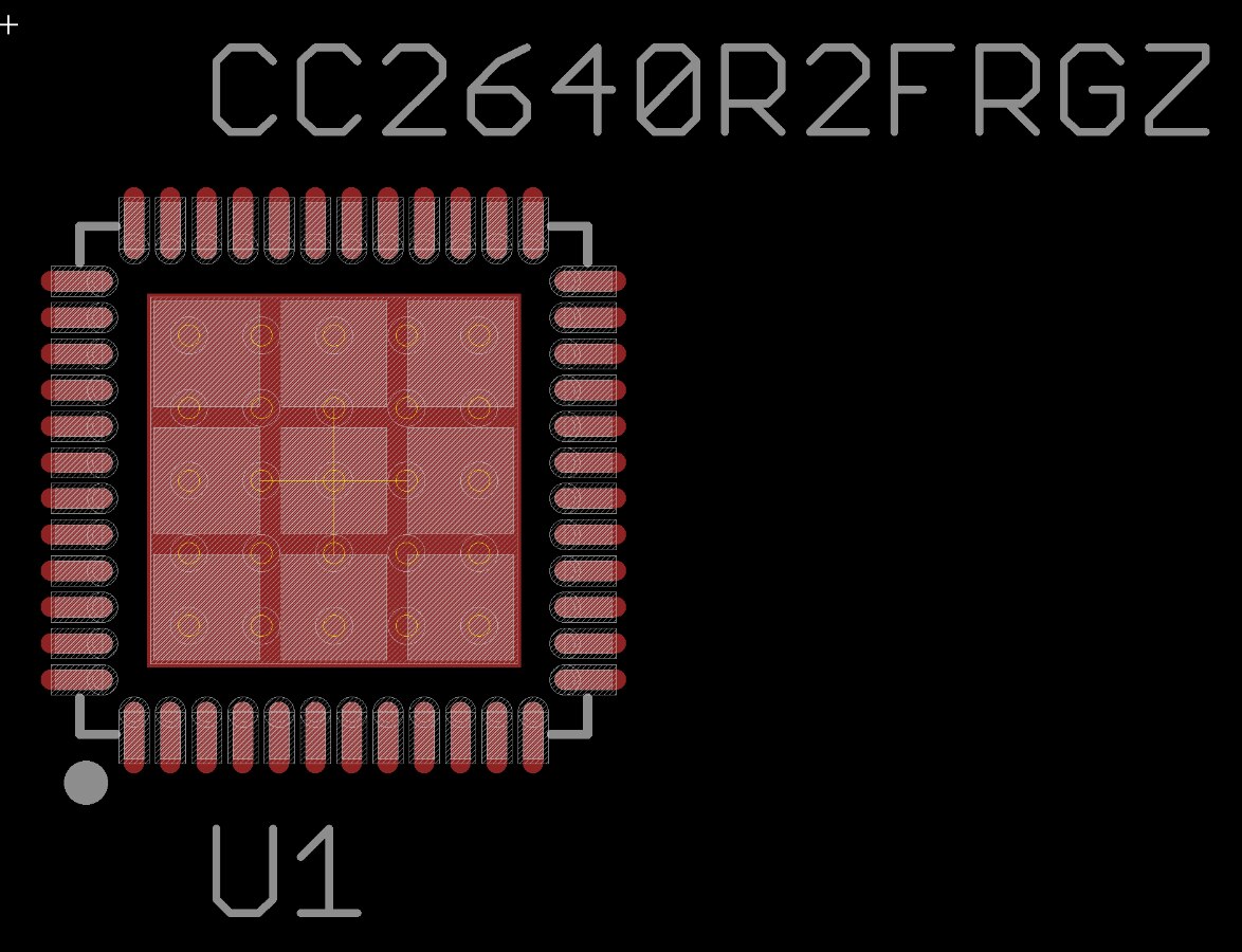
Shaped pads are needed, so they were created by setting the Roundness attribute to 100% on each rectangular pad. I didn’t want solder to travel up the entire pad much beyond the outline of the component, so shapes were drawn on the tStop layer to define the area where the green stuff would be absent on the PCB, and for each pad the automated Stop creation attribute was disabled.


The patchwork of squares in the center pad area in the screenshot above are for the stencil creation, to prevent too much solder paste being applied. For radio chips the vias are mandatory for the ground plane. I will need to consider how to prevent solder wicking into the holes too much. Low-cost PCBs do not have filled via holes. I have a few ideas, but experimentation is needed.


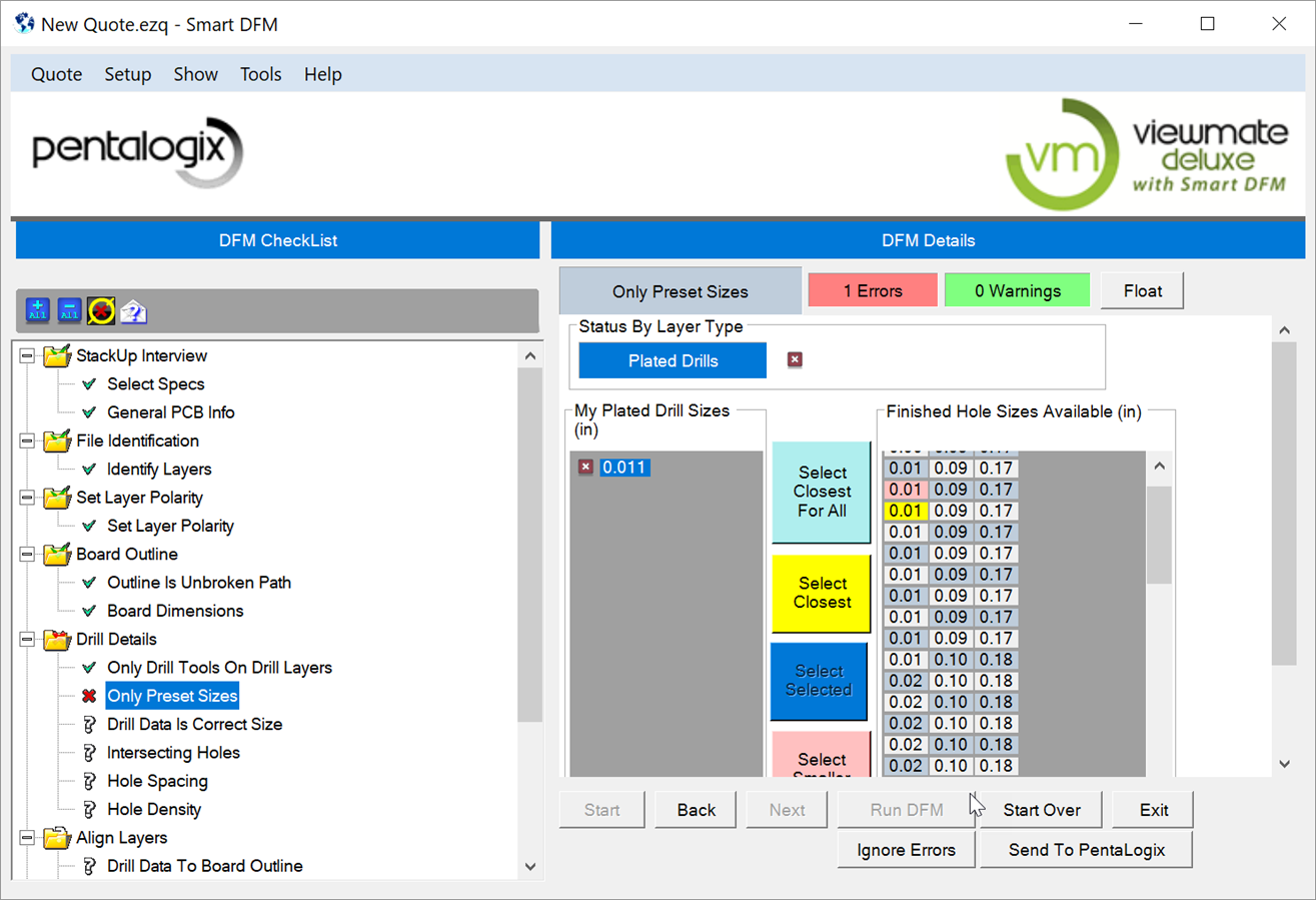
After the part was created, it was verified with a third party viewer, PentaLogix Viewmate. It works really well with EAGLE - just point it at the folder where the Gerber files (generated using EAGLE's computer aided machining [CAM] processor) are stored, and it does its magic.

image


The software can automatically run Design for Manufacture (DFM) rules and inform of errors and warnings that could prevent a successful PCB being manufactured. For instance in my case, it warned that the holes were of a non-standard drill size, which I can easily correct.

image


Component Schematic Entry

As part of the part creation process in EAGLE, the schematic symbol was created too. I used the TI schematic symbol as used in the LaunchPad, as a reference, but with some small adjustments to suit this project.


Since there are many pins (48 plus the center pad), the schematic symbol is split up into two parts; one for input/output connections, and the other for all the remainder connections (such as power, crystal and debugger).

image


Next Steps

The PCB parts entry process will continue as the design evolves. I will also fire up the software development environment, and start getting familiar with working with TI’s operating system (OS) and libraries of useful functions!

  • Sign in to reply

Top Comments

  • shabaz
    shabaz over 7 years ago in reply to genebren +3
    Hi Gene and jw0752 Thanks! I'm not so good at it, since it needs a lot of practice. The few times I've had to use QFN I've not needed vias in the pad, so this will be interesting. I did have vias in a…
  • jw0752
    jw0752 over 7 years ago +2
    Thanks Shabaz, I look forward to following this project. John
  • aspork42
    aspork42 over 7 years ago +2
    Nice job!
Parents
  • genebren
    genebren over 7 years ago

    Shabaz,


    Great update on your project.  Keep up the good work!

    I look forward to seeing how your PCB work goes as I still struggle with making libraries with exposed pads and vias.

    Gene

    • Cancel
    • Vote Up +1 Vote Down
    • Sign in to reply
    • More
    • Cancel
Comment
  • genebren
    genebren over 7 years ago

    Shabaz,


    Great update on your project.  Keep up the good work!

    I look forward to seeing how your PCB work goes as I still struggle with making libraries with exposed pads and vias.

    Gene

    • Cancel
    • Vote Up +1 Vote Down
    • Sign in to reply
    • More
    • Cancel
Children
  • shabaz
    shabaz over 7 years ago in reply to genebren

    Hi Gene and jw0752


    Thanks! I'm not so good at it, since it needs a lot of practice.

    The few times I've had to use QFN I've not needed vias in the pad, so this will be interesting. I did have vias in a heat-sink area once, and the solder dripped out when reflowing. So this time I will try to plug them up, possibly with high-temperature solder first. If that fails I'll leave micropore Kapton tape on the underside to prevent it from going further than the hole depth. But maybe it isn't needed, these holes will be smaller. Anyway, it's all an experiment.. Also, last time I used an oven, but this time I will likely use a hot air tool (and preheat the board).

    • Cancel
    • Vote Up +3 Vote Down
    • Sign in to reply
    • More
    • Cancel
element14 Community

element14 is the first online community specifically for engineers. Connect with your peers and get expert answers to your questions.

  • Members
  • Learn
  • Technologies
  • Challenges & Projects
  • Products
  • Store
  • About Us
  • Feedback & Support
  • FAQs
  • Terms of Use
  • Privacy Policy
  • Legal and Copyright Notices
  • Sitemap
  • Cookies

An Avnet Company © 2025 Premier Farnell Limited. All Rights Reserved.

Premier Farnell Ltd, registered in England and Wales (no 00876412), registered office: Farnell House, Forge Lane, Leeds LS12 2NE.

ICP 备案号 10220084.

Follow element14

  • X
  • Facebook
  • linkedin
  • YouTube