Introduction
With increased connectivity, improved internet speed and ongoing development of machine learning technologies, the Internet of Things (IoT) is transforming almost every aspect of our connected world. The growth has only accelerated after a pandemic year during which we all desperately explore alternatives to face-to-face communication. The result is billions of line-powered smart devices with radios, sensors, actuators, and other connectivity components that constantly need electricity. All of them can add up to a significant impact on worldwide energy consumption. More than ever, compact and highly efficient offline power converters with ultra-low standby power consumption are needed to support the future of IoT.
Today, modern smart homes include digital voice assistants, wireless smart bulbs, or smart thermostats. These devices depend on Wi-Fi connectivity, voice commands, and artificial intelligence to learn and assist in your daily routines. The new smart features are likely controlled by a sophisticated integrated circuit that runs on a low dc voltage. Still, power is distributed via ac power, creating a need to convert from ac to dc. In addition to providing a clean dc power rail to the load, these ac/dc power supplies must also be efficient, reliable, and small. Finding an off-the-shelf power supply that is optimized for your needs can be challenging. Often you are left with more than you need.
Smart devices tend to be small and relatively inexpensive. If you think about the most popular smart devices for your home on the market today, such as the Philipe Hue Light or the Ecobee smart thermostat, they’re often part of a larger network of smart devices throughout the home. If these devices were too large or expensive, consumers would be less inclined to populate their homes with them, and it would defeat the idea of a smart home. For devices like these that will run on low dc voltages, the power supply will significantly impact the device’s overall form factor and cost.
Electromagnetic interference (EMI) filters are one of the main components that take up significant space in a power supply but may not always be needed.
In this blog post, I will design a 220V AC to 5V DC converter for an IoT smart bulb. I will observe the output with and without the line filter.
Design of 220V AC to 5 V DC Converter
In this blog, we will use a low-cost power switch to convert 220V AC to a 5V DC for an inexpensive IoT smart home device like a smart lamp or smart plug. In our test case, we will drive an ESP8266 WiFi module and a relay using the converter output. In the buck converter, we will be required an inductor and we will use it from the kit. First, we will test the circuit without any line filter and then we will test it again with the EMI filter we made in the previous blog.
This is a non-isolated AC-DC conversion with a small form factor, with high levels of efficiency and low standby current, which is perfect for inexpensive small household, office, and industrial appliances that operate as standalone devices or as part of the Internet of Things (IoT). The buck switcher can convert a full-wave rectified, AC input voltage between 85VAC and 265VAC to a nominal 5.0V DC output. Its non-isolated design requires no external transformer and very few external components, saving space and BOM cost. With a no-load power consumption of less than 30mW, the buck switchers are particularly suitable for small appliances that operate in standby mode for prolonged periods when connected to an AC outlet. Its low-power credentials and small solution size also make it appropriate for IoT devices that are always connected but not always active.
Our circuit is based on OB2222, a high-performance, low-cost PWM power switch for a non-isolated DC-DC buck converter. It provides a regulated 5.0V dc output from universal AC input. The typical operating frequency is 40KHz. The datasheet provides the following typical circuit.
The converter uses a single inductor and choosing the right value for the inductor is very important.
From the ROHM Semiconductor application note, I found the following equation for calculating the required inductor value for a buck converter. It is a complex equation and the inductor value depends on several parameters. For details please read the application note from here.
The inductor value greatly depends on the output current and the output ripple. The inductor value can be increased to reduce the ripple ratio. However, this may result in an inductor that is too big in physical size for practical use. So, 'r' is usually set between 0.2 to 0.5. Putting all the parameters in the above equation the required inductor value for our case is around 1mH. We will experiment with a different inductor and observe the result.
The DC output can provide a maximum of 300mA current with is enough for many low-power IoT smart home devices. I made the following final circuit for my experiment. I used a 1mH inductor for my design. The ESP8266 required a 3.3 V supply. So, 5V output from the buck converter is reduced to 3.3V using a linear regulator.
I made the first prototype with a handmade PCB for only the power supply unit. The circuit also contains the 3.3V regulation part.
Testing The Circuit
[Note: The following experiments used high voltage. Working with high voltage can be lethal. I did those experiments very carefully. So, do it at your own risk. I recommend using your own protection and making sure you are not making any mistakes.]
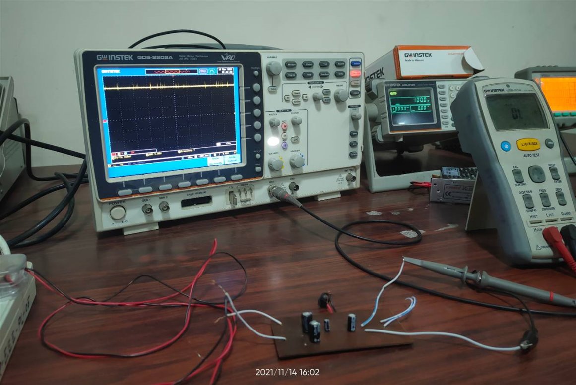
First I measure the output voltage with a multimeter and then I observed the output in an oscilloscope to watch the quality of the DC and find some high-frequency noise in the DC output. No EMI or line filter was attached to the circuit.
Oscilloscope screenshot for the above connection.
I thought the noise is generated for bad PCB quality. So I decided to make a PCB from any professional PCB service provider.
So, for getting a clean output from the above circuit I designed a PCB layout for professional PCB fabrication. The PCB layout is designed in EasyEDA. This is a double-sided PCB. I used a MOV on the input side to protect the circuit from high voltage surges.
The following image shows a 3D view of the PCB.
A printed PCB image is given below.
After placing and soldering all the components the circuit looks as follows. The Inductor L2 in the circuit is one of the most important components here. I tested the circuit for different inductor values and find that 1mH is the optimum value for the circuit in terms of output voltage, inductor current, and output current. So I soldered a 1mH inductor in my final circuit.
Experiment with Final Circuit with Different Inductors
The first work is to measure the inductor's value using an inductance meter. I used an LCR meter to measure the inductance of all the inductors.
I note down all the inductor values on paper.
I used inductors from 100uH to 1100uH for testing the performance of the circuit.
Measuring the Bourns high current choke the biggest inductor I tested in the circuit. The Q of the inductor was measured as 5.11.
Measuring Bourns Shielded construction radial RF choke. This inductor has the highest Q (8.19) of all of the inductors I tested here.
All the inductor's values are recorded on paper.
For easily connecting different inductors in the PCB I soldered two female jumper wires in the two pads on PCB. Then I measured the output voltage by adding a different inductor each time and recorded.
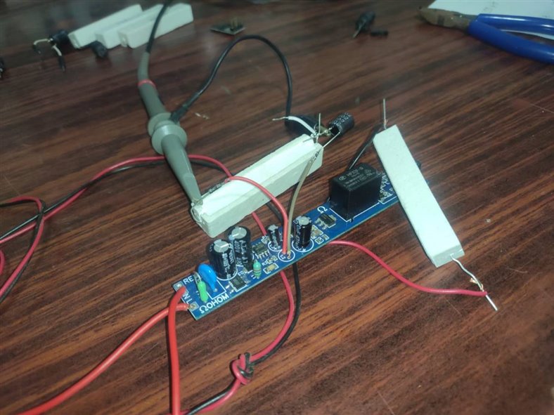
For measuring and observing the inductor current in an oscilloscope I added a 1ohm 5W resistor in series with the inductor. I added another 10ohm, 5W resistor as load. The following image shows the inductor current waveform when Bourns 1mH inductor was placed in the circuit.
The following image was taken when the 555uH inductor was connected to the circuit. It shows more switching ripple than the previous image where a 1mH inductor was used.
Oscilloscope screenshot of the inductor current for the above setup.
The following images are for 10uH and 4uH inductor respectively.
The following image shows the inductor current when the EMI filter is connected to the input side of the circuit.
Findings & Observation
The following table shows the output voltage of the buck converter for different inductor values.
From the above table, it is clear that output voltage is directly related to the inductance. The output voltage is higher for a lower inductor value.
The following image shows the inductor current waveforms for different inductor values for the same load.
The following table shows the inductor current for different inductor values with the same load. From the table, it is clear that a larger inductor allows a lesser current for maintaining the same load current. The current ripple is also lower for a larger inductor. But there is a trade-off between inductor value and the physical size of the inductor. Price is also higher for a large inductor. So, we have to compromise among all the parameters, and for my circuit 1mH is the optimum inductor value.
EMI filter reduces the ripple of output voltage and inductor current but does not worth the extra money and size of the circuit. So, it is not mandatory if there is no certification issue.
Watch the following short video clip to see how the EMI filter reduces the EMI noise for the buck converter.
The Final Device
The following picture shows the final 220 V AC to 3.3 V DC switching converter using Bourns Inductors when it is in operation.


Top Comments
-

michaelkellett
-
Cancel
-
Vote Up
+1
Vote Down
-
-
Sign in to reply
-
More
-
Cancel
Comment-

michaelkellett
-
Cancel
-
Vote Up
+1
Vote Down
-
-
Sign in to reply
-
More
-
Cancel
Children