


It’s been a while, members of the element14 Community! I’ve been away for a while due to health issues, but this contest marks my (attempted) return. I guess I really do need to “light up my life”, thanks to Würth Elektronik and their WL-ICLEDs. But as luck would have it, I’ve already been stymied by contracting the flu just as the build period began alongside the return of temporary vision loss in my left eye making things a tiny bit tricky. Nevertheless, I’m now playing catch-up after finishing a few other commitments (which include a lot of things happening on my personal blog including a review of a PCB-oriented thermal camera).
Which has me thinking – what is one of the most common issues when reverse-engineering or troubleshooting PCBs under a microscope or a macro lens?
Proposal
When examining PCBs or surface mount components with a microscope or a macro lens on a DSLR, the tracks underneath the shiny glossy surfaces and shallow markings on IC packages can often be hard to visualise. To try and get the to show often takes a lot of effort adjusting goose-neck LED lights to get just the right angle and brightness to avoid “hot-spots” on your images and to maximise contrast.
In this project, I propose using the new WL-ICLEDs from Würth Elektronik to build a better light source that can be used with a microscope and/or a DSLR camera. This would be a ring of WL-ICLEDs which can be adjusted for brightness to avoid wash-out, but also in colour to choose one which maximises contrast given a particular board colour, to aid in following traces. A key benefit of the ring design would be the ability to selectively turn on ranges of LEDs, allowing for the angle of illumination to be changed electronically, thus providing more repeatable imaging and avoiding the fatigue and wearout of mechanical goose-neck LED designs. Furthermore, a second linear array of WL-ICLEDs would be used to construct an edge-firing light for use in imaging surface irregularities or particularly challenging markings which require very oblique lighting angles.
Unboxing

The box of challenger parts arrived for me with no issues – thanks TNT/FedEx and element14.
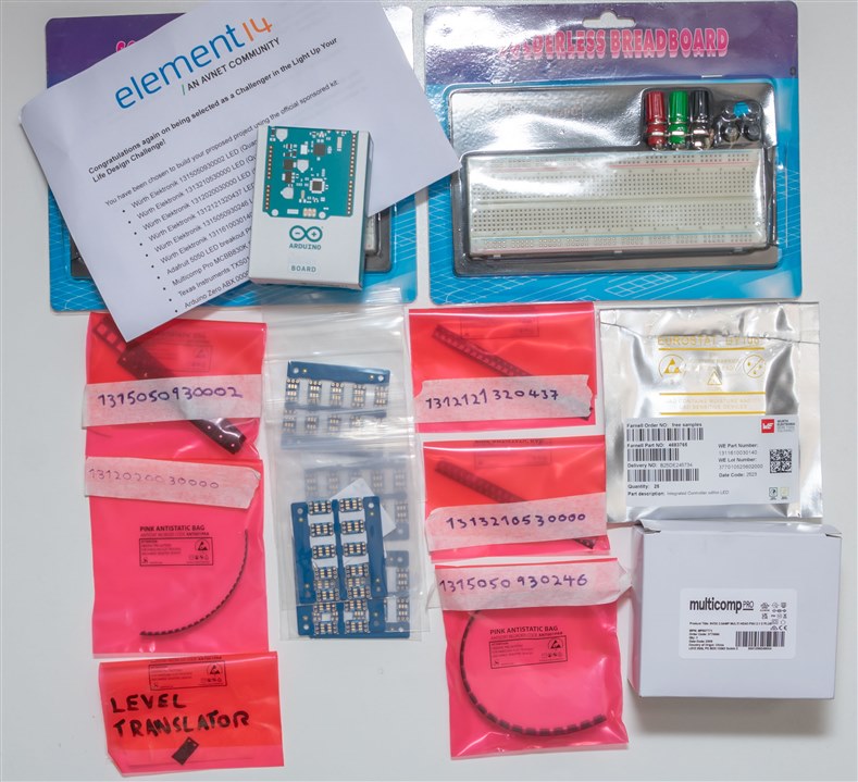
Inside was all the promised goodies – let’s take a look at closer look at all of them.


The all-important challenger’s letter that lets us know what’s in the kit and what to do. Staying social? Well, um … sorry, I think I’ve already failed on that one!
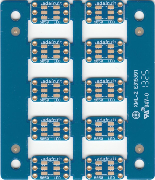
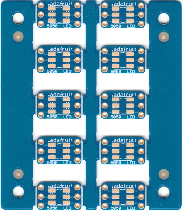
The Adafruit 5050 SMD LED breakouts come as a nice 0.8mm thick gold-plated finish double-sided PCB. While you won’t likely be able to use both sides of these breakouts at the same time, at least if it means you screw up on one side, you could perhaps use the other. The design is somewhat genius – you’ll see what I mean in the next posting perhaps, but keeping things together as a panel with rails and relatively light V-scores means that the breakouts can be more easily assembled – otherwise there’s literally nowhere to secure the fingernail-sized breakouts during soldering. This will be good for the 5050-size LEDs, but the others are going to need PCBs designed ...
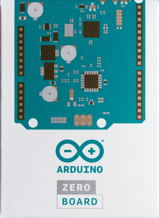
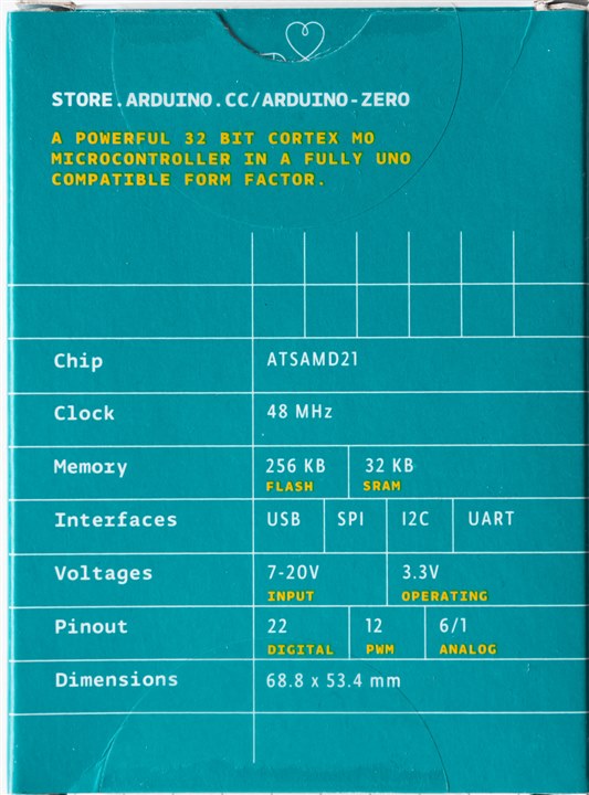
The Arduino Zero is a relatively new board to me. From looking at the specs, it almost looks to be an Uno-footprint with an MKR “heart” – the 3.3V-based 48MHz ARM Cortex M0+ ATSAMD21 microcontroller.

I do like that after all this time, the packaging still remains familiar and the products are still Made in Italy – but I wonder how the recent Qualcomm acquisition of Arduino will affect its future.
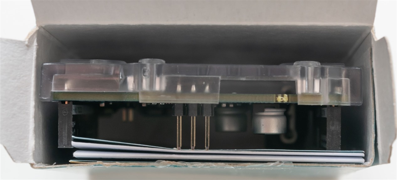
Time to take things out of the box …
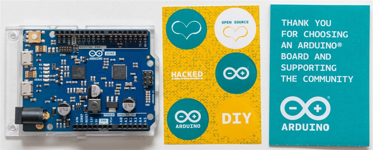
I can’t say I’m too fond of the stickers – and the board seems a more ordinary blue than the teal-green-blue of the Unos of old.
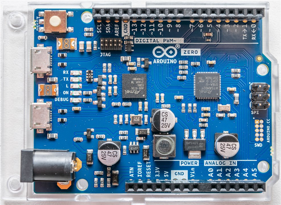
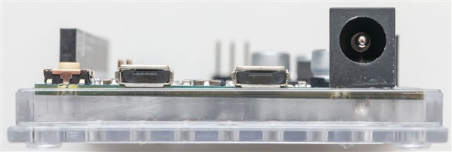
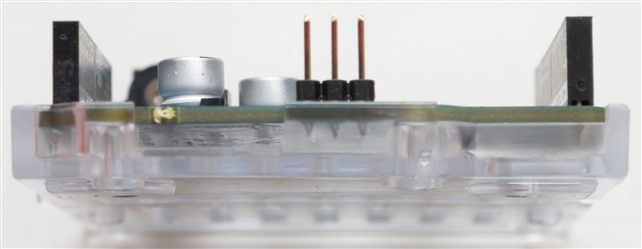
The board is relatively busy though – two USB micro-B connections is a new thing to me (looks like this means it’s got an onboard debugger), as is having a JTAG header. As for why this board was chosen, I suppose part of the magic may well be the switching buck regulator that’s on this board. Most Arduino boards in the past used just linear solutions, but this one has a LM2734Y that has a 1A rating, so with the lower losses compared to previous linear supplies, this should mean more current available for LEDs to consume when supplied by the barrel jack supply.
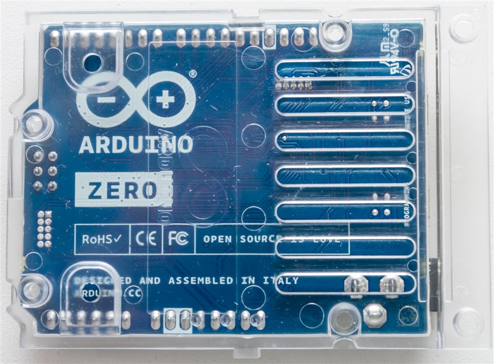
I like the fact the plastic tray is still included – no more worrying about shorting out on the mat or bench wire scraps. That’s definitely something the clones don’t have.
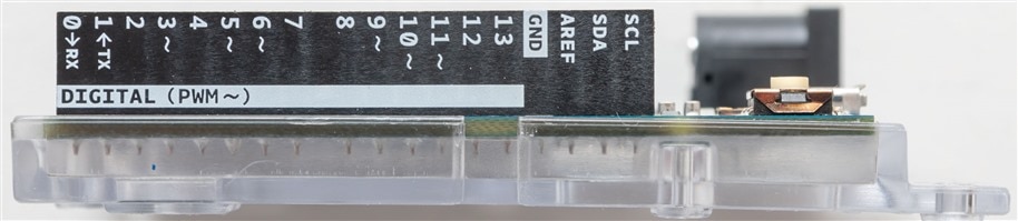
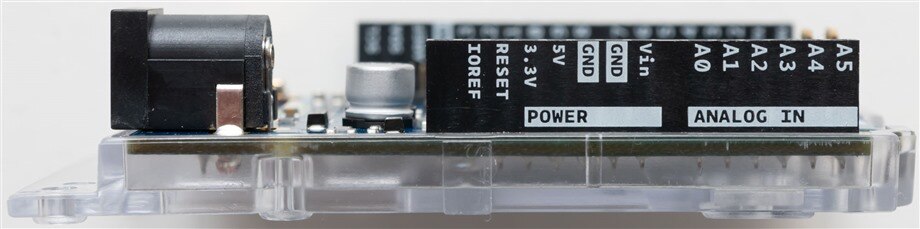
Other benefits include the labelled headers.
While most ordinary USB ports can source about 500mA, USB 3.0 ports should be able to provide 900mA and some USB DCP can do as much as 1.5A. As a result, while the barrel jack supply is perhaps nice, it might not be necessary if a powerful port and a good cable is used. That being said, it just occurred to me that a cable is not included … and my house is mostly USB-C now. Definitely a “first world problem!”
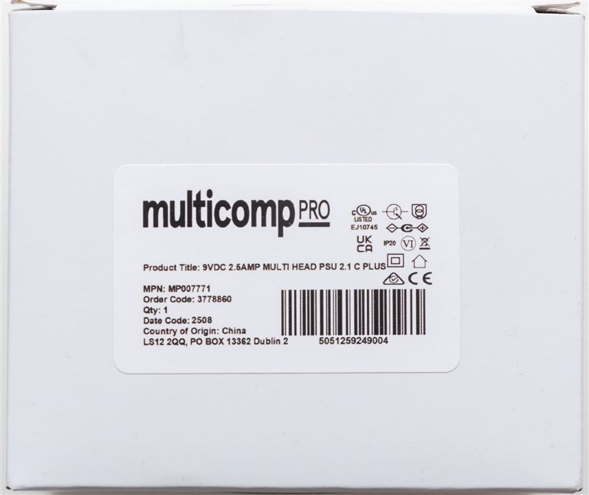
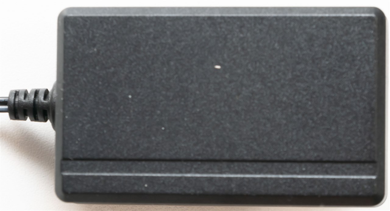
Speaking of power supplies, element14 have provided one of their house-brand “Multicomp Pro” supplies. This is a 9V 2.5A supply with plugs to suit all countries, carrying a wide array of certifications including the Australian RCM (good news for me). It has a part number of MP007771 and is Made in China.
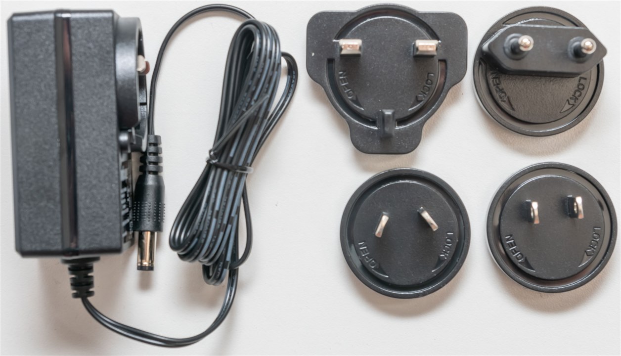
Four heads are provided in total, none are pre-fitted.
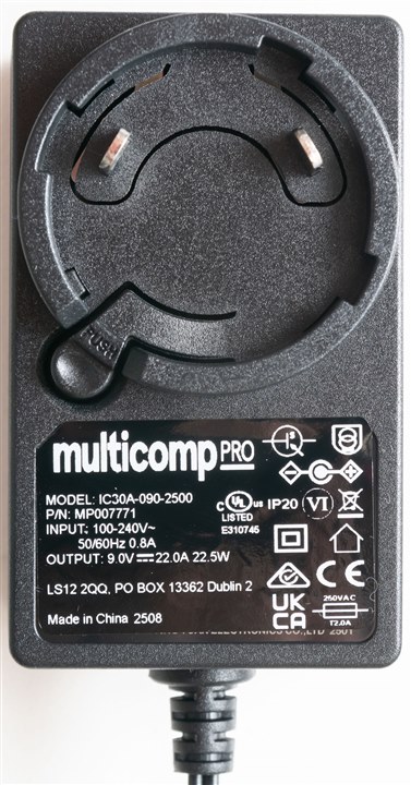
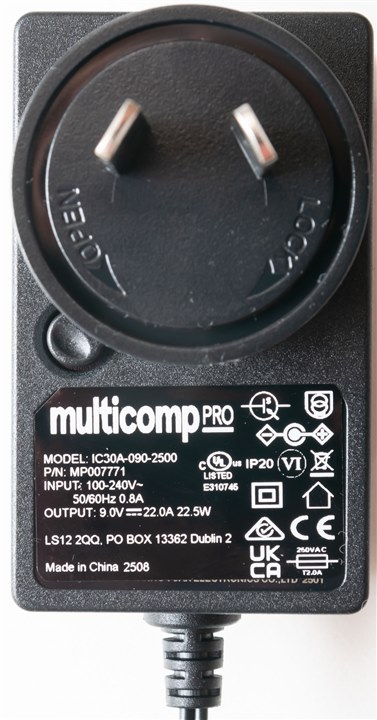
The heads twist-lock onto the base and then the supply is ready for use. But I had a big laugh – the branding label they’ve affixed is obviously a label over the original printing, but it also contains a significant error – 22.0A. This is definitely not a 22A supply. It’s 2.5A, but obviously, this typo wasn’t picked up on.
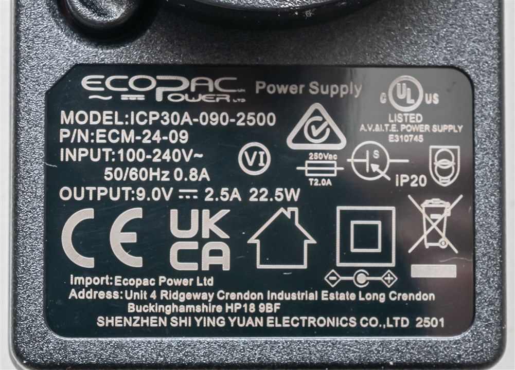
Seeing as it’s obviously a label, I peeled it off to reveal that it’s an Ecopac Power branded product, but that is a product of Shenzhen Shi Ying Yuan Electronics Co. Ltd.
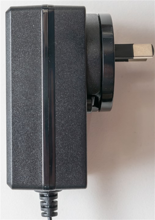
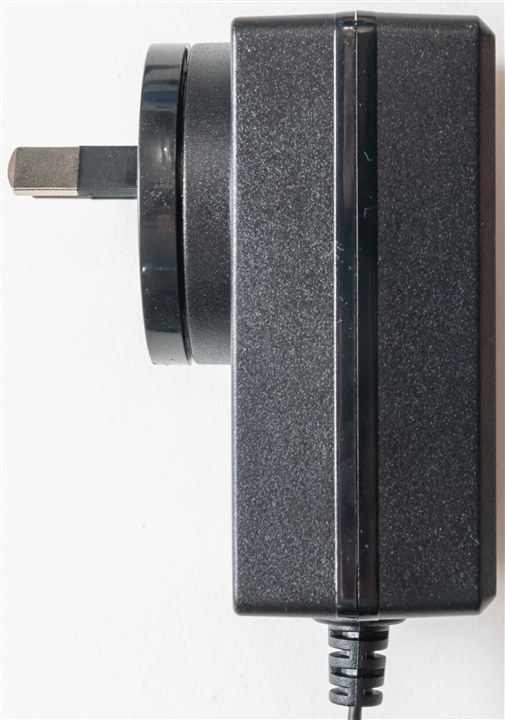
Regardless, the adapter has a relatively slim profile – doesn’t block adjacent power outlets which is nice.
No indicator LEDs – that probably helps when it comes to chasing higher efficiencies and keeping costs down.
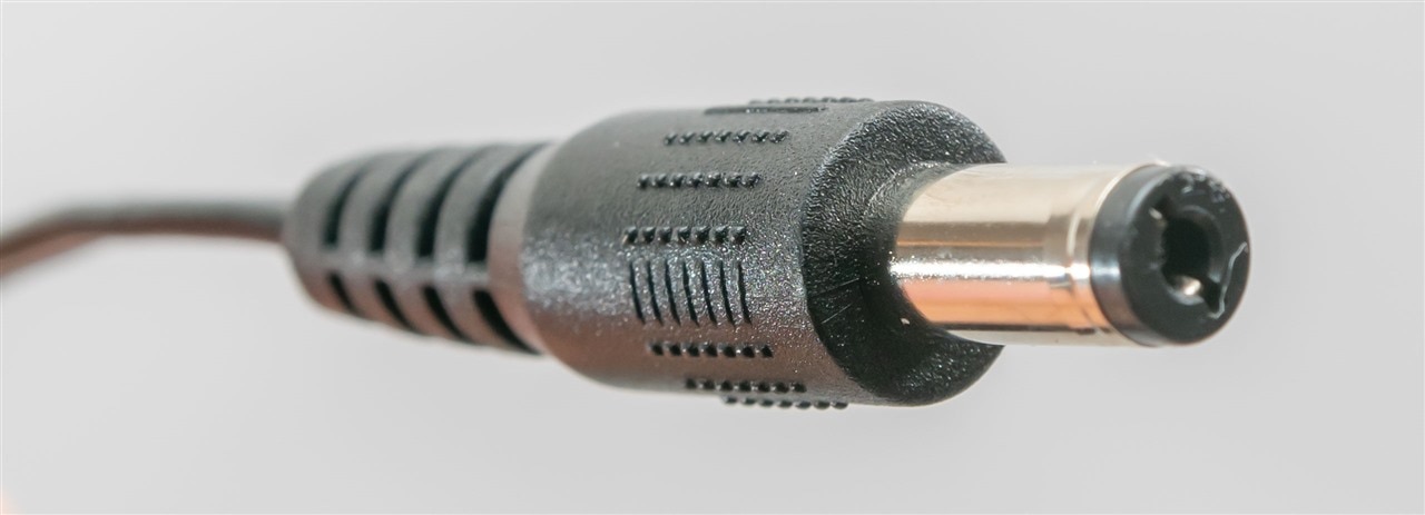
The cable is terminated in a 2.1mm ID plug, ready for use with the Arduino Zero above.
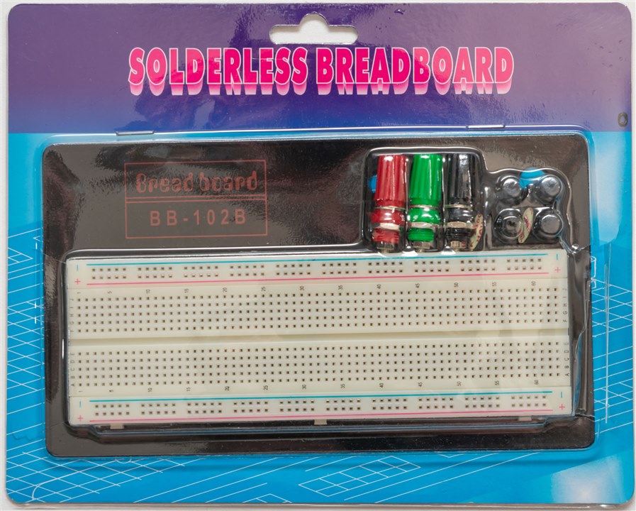
Next, we have the breadboard. In prior years, I’ve had a couple under the “element14 Presents” branding (just a sticker) but these came without.
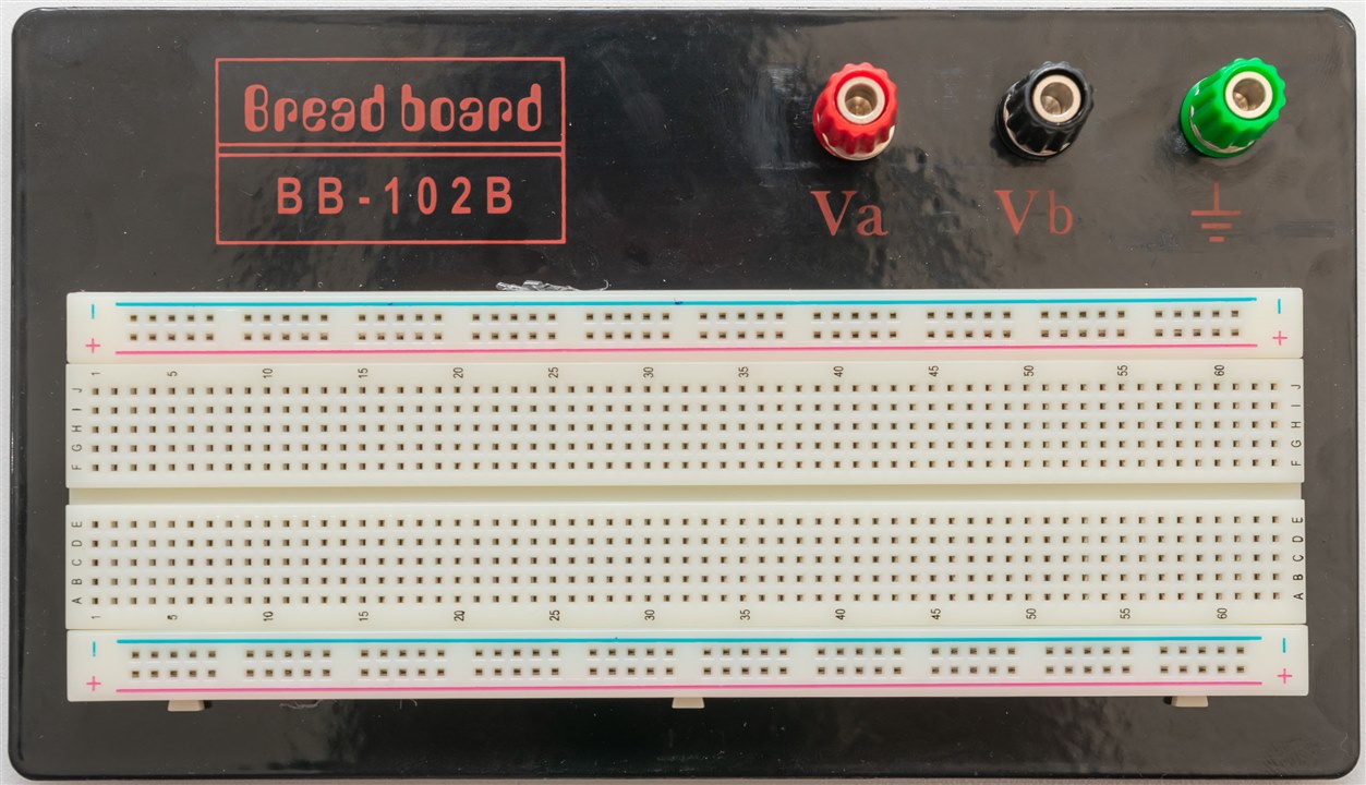
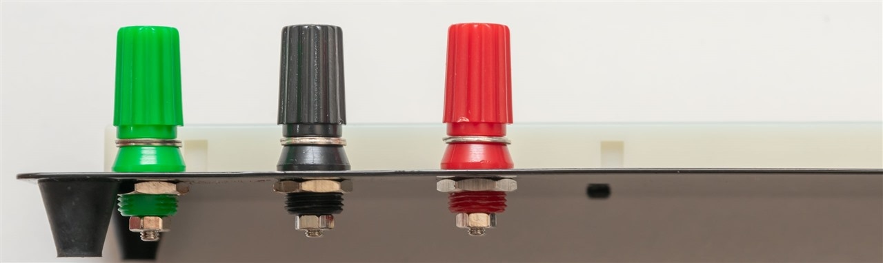
Some minor assembly is required – fitting the banana jacks, assuming that you would like to use them.
They’re nice breadboards – but the feet often lose their stickiness and get lost, resulting in something that just doesn’t sit flat on the table.
A Closer Look at the LEDs
You might have noticed I haven’t said anything about the semiconductors – well, that’s because I needed to break out the microscope to get a good look at them.
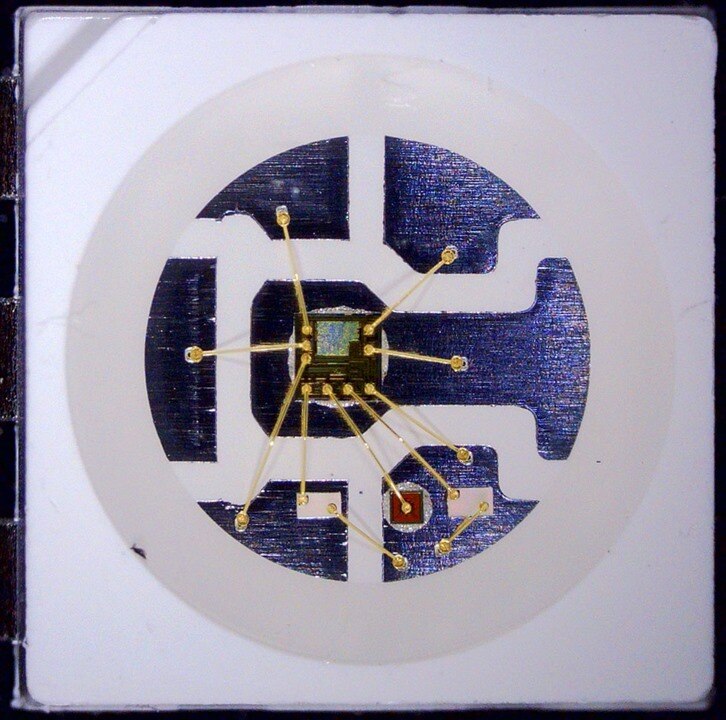
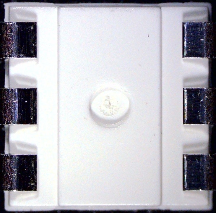
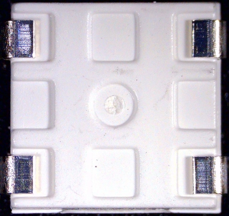
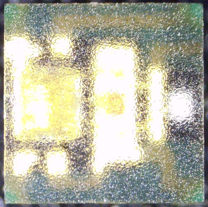
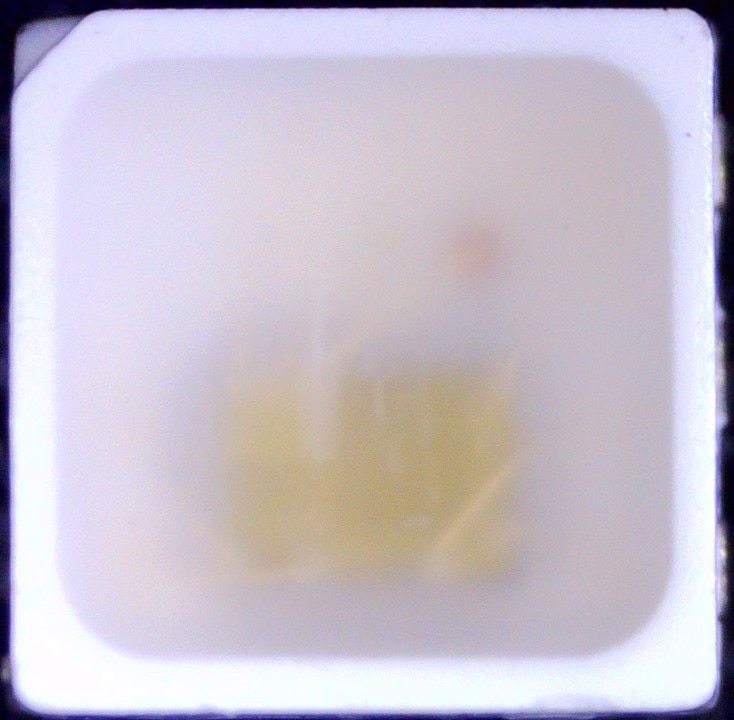
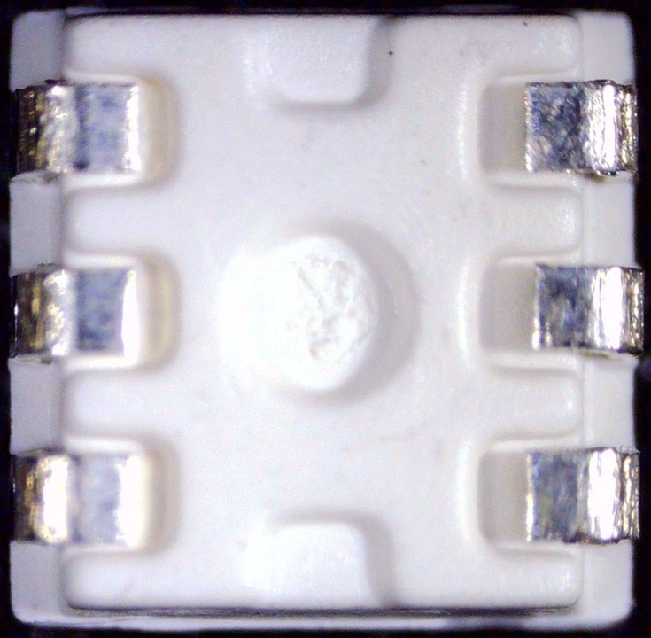
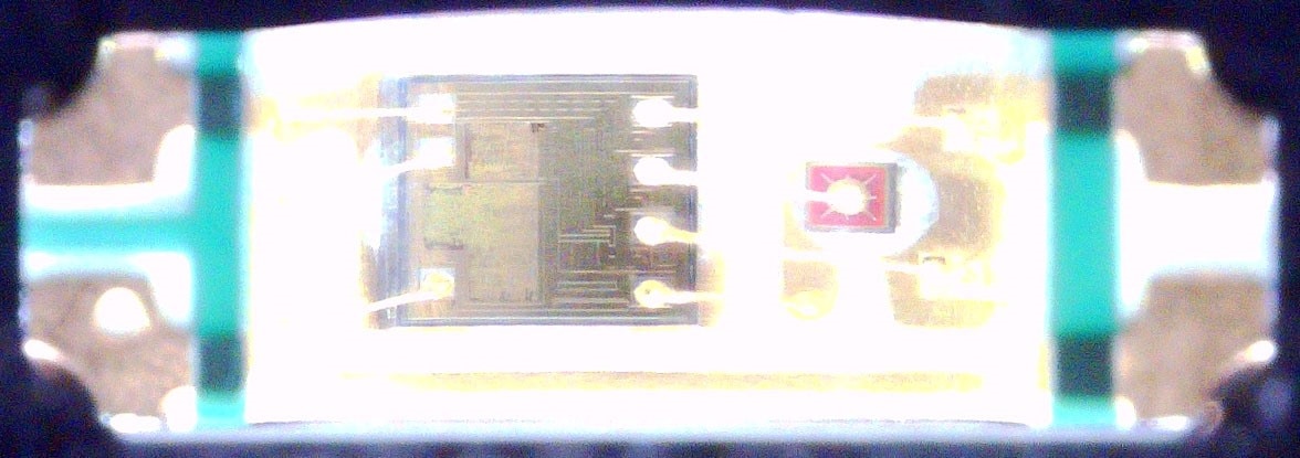
First off-the-batt is the 1315050930246 (Würth Elektronik loves long part numbers) which is a 5050-size LED. Looking at this, it looks similar to APA102-based (or colloquially known as “Adafruit Dotstar” or “Sparkfun Lumenati”) LED. These use a synchronous SPI-like bus (clock + data) in a daisy-chain configuration, thus requiring six contacts.
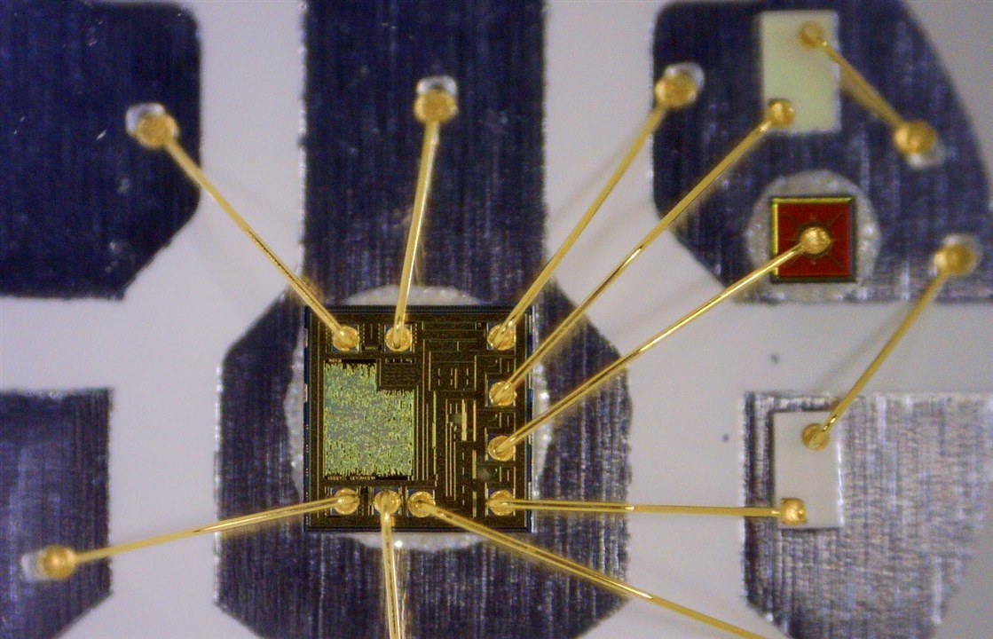
A closer look through the optically clear packaging material shows the large controller IC compared to the three small LED chips along with their gold bond wires. The bright area is probably the digital logic, while the darker area that surrounds it likely be the transistors, resistors, capacitors and diodes that drive the outputs.
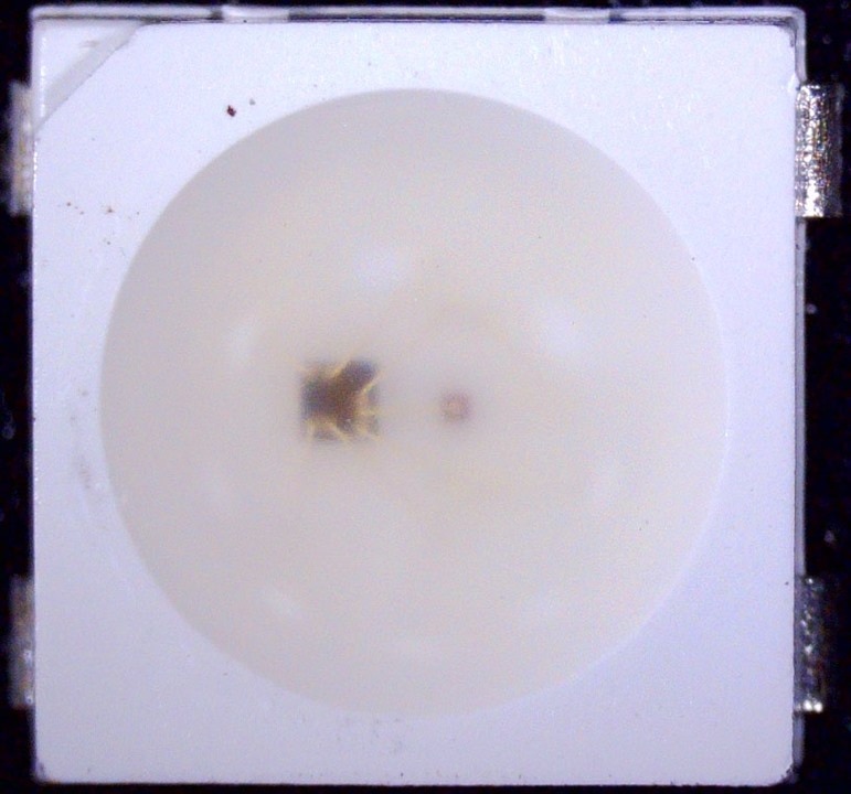
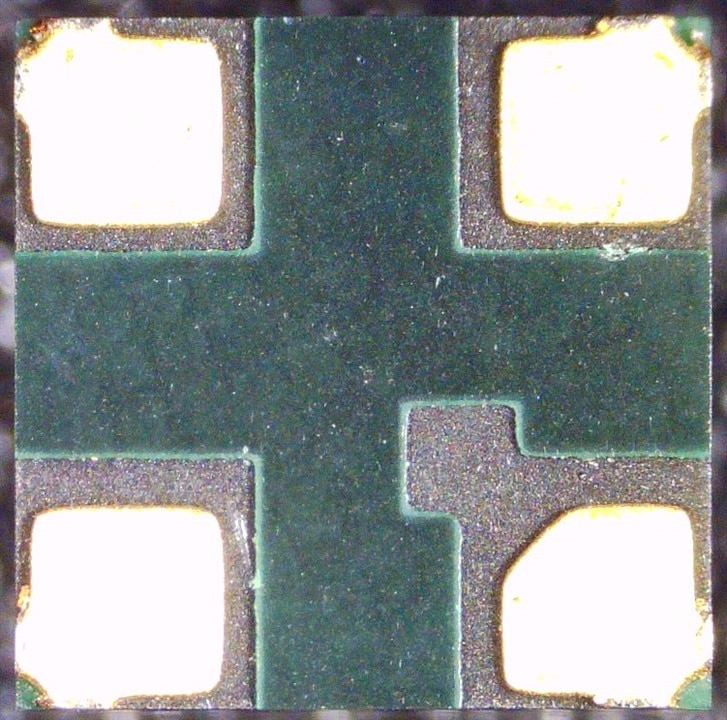
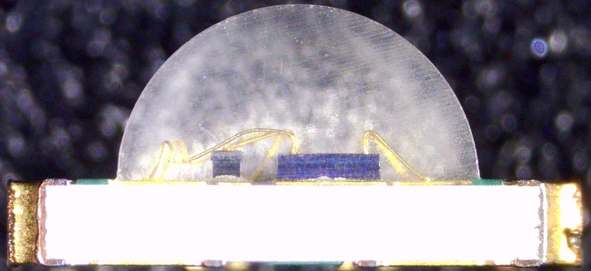
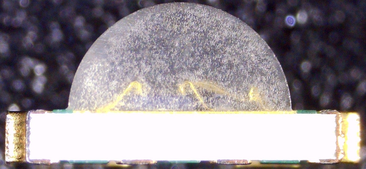
The next is another 5050-size LED, the 1315050930002. This particular LED instead has four connections, as it uses a one-wire daisy chain protocol, likely similar to the ubiquitous WS2812B (also colloquially known as “Adafruit Neopixel”). This particular signalling protocol is much more sensitive to timing, being an asynchronous protocol and likely operates at a lower speed compared to the synchronous protocol above, limiting refresh rates. The optical compound provides diffused light in this particular type, so we cannot see clearly inside, but it looks to me that the die in this design is smaller than the other.
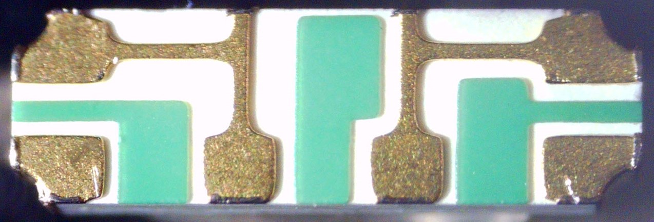
This type is a smaller 2020-size LED, with part number 1312020030000. It too uses a single-wire daisy-chain bus as the 5050-size version above. It is packaged in what looks to be a clear resin with a texture to provide some diffusion of the light.
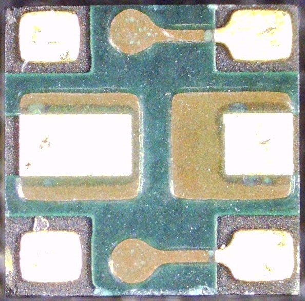
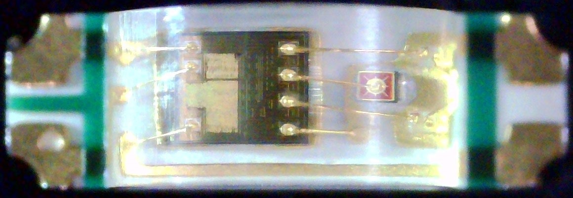
This is the two-wire synchronous version in 1610-size, part number 1311610030140. At this size, the inside of the package really looks like it's getting cramped!
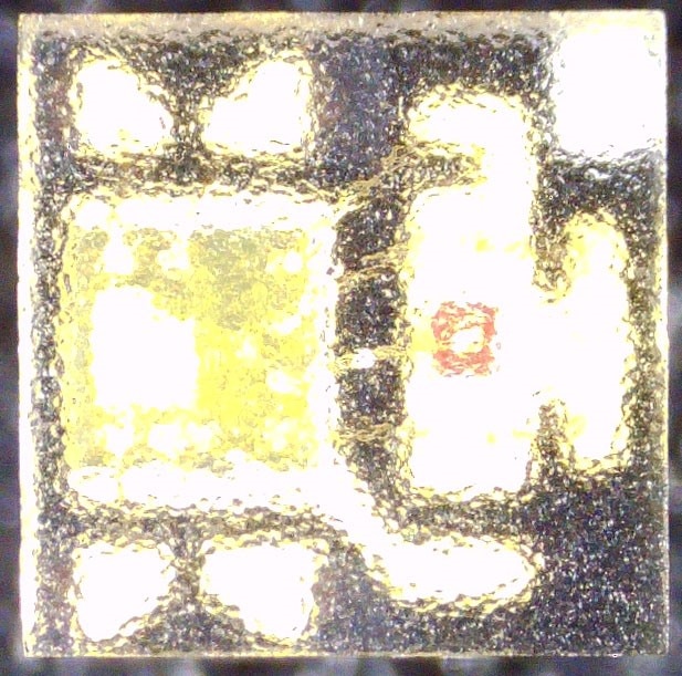
There is a 2121-size LED with a part number of 1312121320437. This particular chip has six connections, but operates using a single-wire bus – the extra connection is named “BI” and appears to be a bypass connection. This is a special feature of later WS2813 type LEDs that helps guard against one bad LED in the string from taking down the whole array – the bypass connection is connected to the data in line of the previous LED. This one is likely compatible in a similar way, although I have not delved into the timings and data formats to confirm. The shape of the shell seems to ensure this LED has a more rectangular radiation pattern, compared to the circular ones of the 5050 type.
Finally, there is the 1313210530000 which is a 3210-size single-wire bus LED which is designed to be mounted on its edge for edge-firing applications.
Being a smaller LED, the fit is pretty tight in there – the thickness of the IC and the LED chips is fairly similar and it’s beautiful to see the gold bond wires connecting the two together. The substrate and connection pad patterns are quite interesting – it seems to suggest an upward firing position may even be possible (although not recommended).
Finally, there is also the level translator (or level shifter).
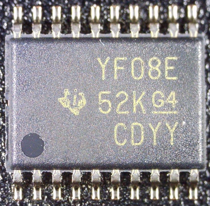
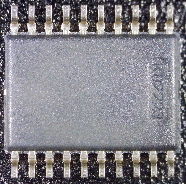
We were provided with just a single Texas Instruments TXS0108EPWR 8-bit bidirectional level translator chip. Because of the package of the chip, it’s not really friendly for use with breadboards, so a breakout would have been nicer. I might substitute my own level shifter instead for breadboard purposes and use this one for a final PCB – but eight channels also seems a bit of overkill but perhaps it was intended so we could run multiple buses of all variants of the WL-ICLED at once (with two channels required by the “clocked” and one channel required by the “clockless” variants).
Conclusion
In this post, I’ve introduced the concept that I proposed as a part of this challenge, taken a look at all the components of the challenger’s kit in detail and broken out the microscope to look closer at Würth Elektronik’s WL-ICLEDs. From an initial glance, it seems the LEDs are somehow similar to the WS2812B/WS2813 single-wire (timing sensitive) asynchronous daisy chained bus and APA102-based two-wire synchronous daisy chained bus LEDs and may even be intercompatible due to the claim of being possible to use with the FastLED library.
The next challenge will be to get them up and running, which involves SMD soldering – a key aspect which may have put off some potential applicants from attempting this particular challenge. Hopefully, I can show how it can be done successfully even with relatively minimal equipment – even though such parts are optimised for mass production workflows.
Stay tuned for further instalments as I try to prototype and test a breadboard solution before I consider designing a PCB. Given the time that remains, it would be quite challenging to have the PCB done in time, but if things pan out, I’ll still be giving this a go because this is a problem I’d really like to solve!


