


Hello. I welcome you to my second forum post as part of Light Up Your Life Challenge!. In this forum post I will share my experience with PCB design and soldering LEDs.
For testing PCBs, I designed 3 PCBs. One for each type of LED I will play with. PCB for 1315050930002 (which is classic one; compatible with WS2812Bs) I actually made few years back, originally intended for WS2812B LEDs. So, at this step I tested compatibility for first time – 1315050930002 matches PCB layout exactly. Remaining two PCBs for 1312121320437 (6-pin LEDs with 48-bit single wire protocol) and 1311610030140 (6-pin LEDs with two wire SPI-like protocol) designed from scratch. I focused common best practices. I dedicated 1 layer for GND plane and VCC wire I made stronger. Signal wires are thin. Here are PCBs as I designed and route them.
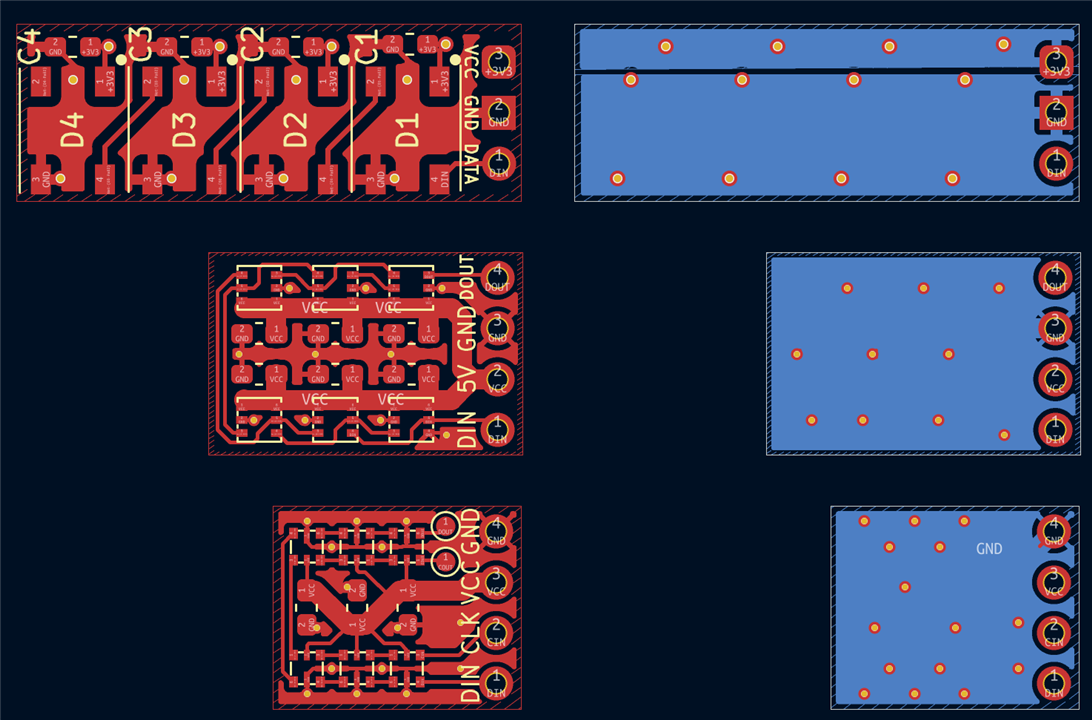
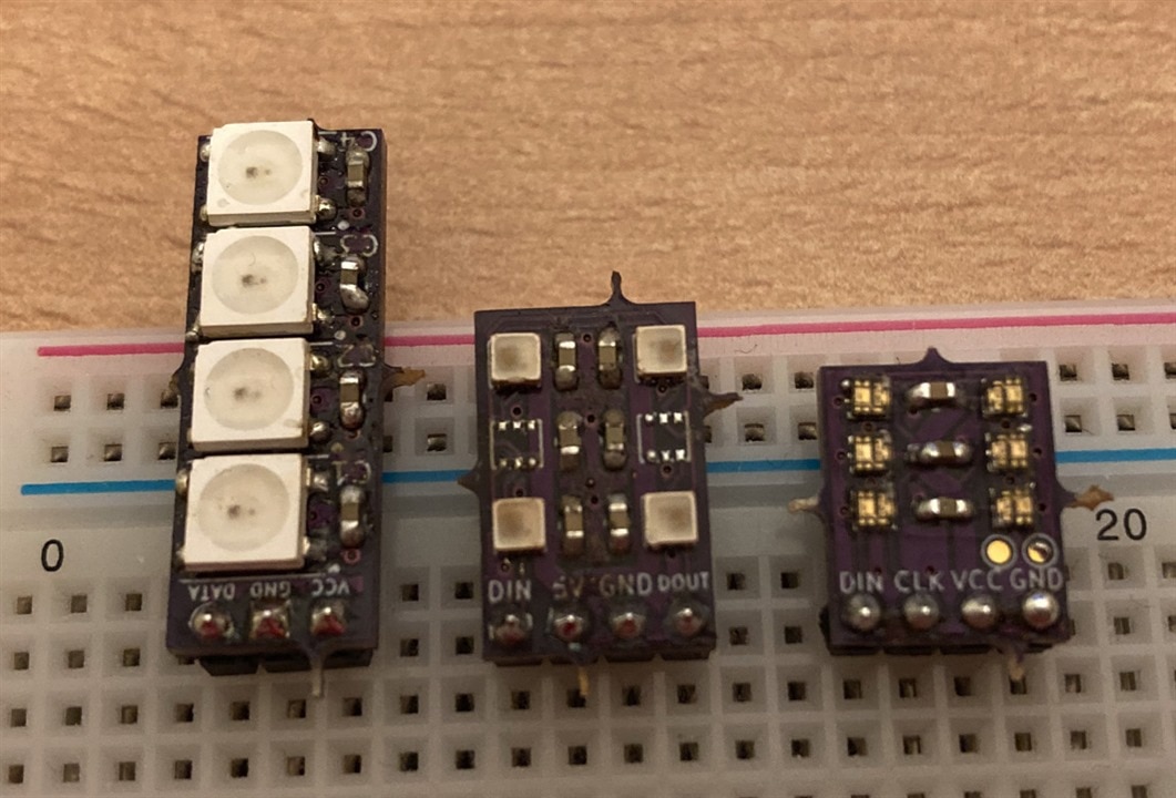
For making it simple I will refer LEDs as largest (Würth number 1315050930002), medium (1312121320437) and small (1311610030140) in this forum post. Sizes proportionally apply to PCB sizes in Kicad screenshot above.
Tracing wires was quite easy. All LEDs are designed in a way that it is possible to route signals reasonably well even on 2-layer PCBs. DOUT signals of LED connect to DIN signals of LED without need to cross anything. This apply even to medium sized which has BI PIN which is basically signal from second previous LED. It is used as a fallback for case when previous LED broke. In that case it does not receive signal from previous, but from second previous and continue operate. Technically you do not need it and you can just ground that pin (this is actual case of first LED in chain). I routed it and PCB look nicely even when it is routed. I added 100nF capacitor to every LED, except for smallest. In case of smallest, I added one cap for 2 LEDs to make PCB compact. At soldering time, I actually, replaced exactly one 100nF cap per board by 1uF. In case of my older PCB for classic LEDs (largest), I routed VCC as stripe on back side. On newer two PCBs I routed in on top section in between two columns of LEDs.
Soldering
For soldering, I used solder past and hot air approach. I applied solder paste manually (without stencil) inaccurately like this:
Placed components onto it like on following picture. I do not like that pin 1 marker is hardly visible on Würth LEDs. WS2812 has bigger marker. On Würth LED it is barely visible and I had to use magnifier glass. But on other hands Würth mention how is chip placed inside package, so it can be aligned just by observing internals of LED without checking corners. This I used for triple checking. At that point it looked like this:
And then I heated it by hot air.
Actually, the biggest mistake was to use more than 2-year-old solder paste. It did not go well. Most of flux dried out. I had really hard time. Components did not fit at right position. I had to manually align them when heating. Because layer of solder paste was highly non-uniform, some joins were very fat, some were unconnected, some were shorted. It did not auto balance like I have seen in my previous hot air attemps. In case of classic LEDs which are quite large, I manually fixed all these by solder pen. In case of small and medium I tried to push them to the PCB. This pushed lot of amount solder from bottom of chips, but in case of medium sized it shorted lot of pins of LEDs. It was visible because these LEDs have visible pins from sides. Interestingly, the easiest were the smallest one. I pushed them, this eliminated over-solder from bottom of LED and additional solder remained as solder balls on side of chip. these I removed by pen solder then. The hardest was the middle-sized one. I had to desolder them all, remove all solder paste from both PCB and LEDs and choose alternative strategy. Alternative strategy was that I applied some amount of tin to pads by pen (but not placed LEDs with solder pen). Then heated again by hot air and placed LEDs one by one into tin applied by solder pen previously. It was still quite hard because amount of tin which I applied by pen soldering was quite low, so I had hart time to place LED and push it to the tin. Most of the time they flown away because of “wind” from hot air solder.
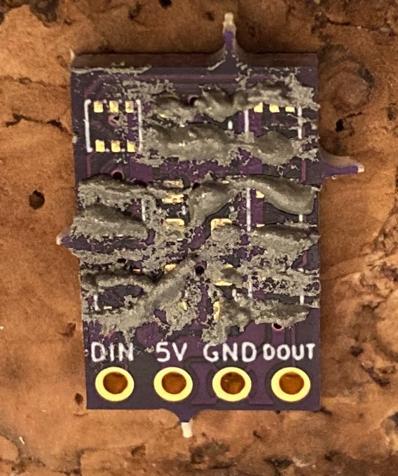
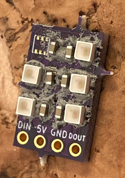
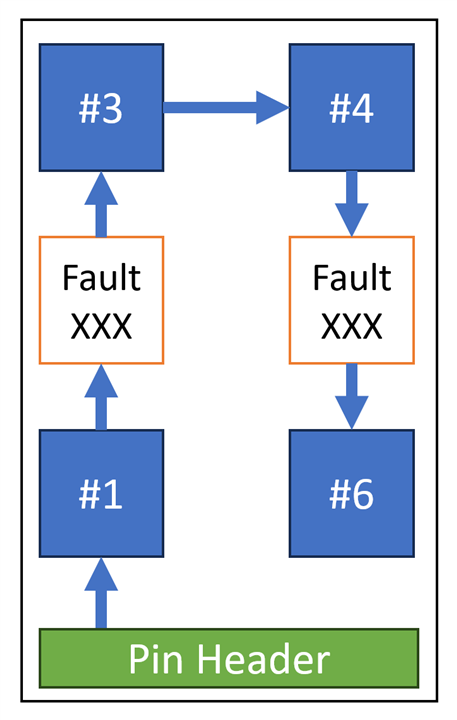
Luckily the hardest LED is the only LED which has BI pin which allow operation of chain even one LED is broken. Missing LED can be considered as “broken” because it behaves in the same way (well actually there are other modes of failure like short circuit, but for simplicity let’s consider missing led equivalent to broken LED). As you can see on the photo above, I intentionally missed one when playing components. Let’s call it sophisticated faulty LED simulator. But later when soldering I broken one more, so I ended up with only 4 LEDs. Main requirement is that there are no two faulty LEDs consecutively. When I was reworking this PCB, I moved the LED to the corner and missed LEDs are actually middle one:
Schematically that PCB looks like
Finally, it looks like:
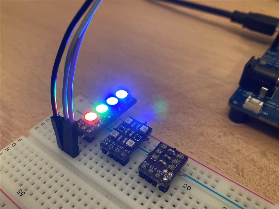
I already test classic (largest) ones because I recently did Halloween Project14, so I have firmware capable of generating signal right at hand. It works!
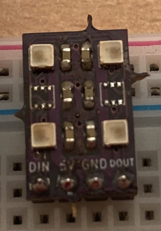
Remaining I tested only by multimeter. I tested that there are no shorts between pins and that ESD diodes between VCC, GND and signal pins are detectable. They are. Still there may be some bad joints on data signals between LEDs. It would be better to place some test point on these signals, but I did not get it at PCB design time.
For testing others, I need to modify firmware. In next forum post I want to spend some time and play with middle sized LED and test that BI pin feature actually works. In other words, I will test my sophisticated faulty LED simulator. And finally, one lesson: If your only solder paste is several years old and dry, buy new with LEDs.
Next forum post: Misaz’s WL-ICLED experiments: Testing BI pin