


What is Vivado
- IDE to Synthesize and Analysis of HDL/Verilog Language
- A single tool to Write, Compile, Simulate and Program
Hardware Training Summary
Lesson 2: The Case for a System-on-Chip
Case for SoC : Why do we need SoC
- Processor utilization > 90%
- Quelength > 2
- Multi Proc System, Time >50%
- Intensive recurring task :
Effect of Poor Performance Processor
- Data Latency
- Delayed interrupt handling
- Lowered data throughput
- Sequential processing limits performance : Parallel Processing is Efficient
- Parallel processing can be done using FPGA
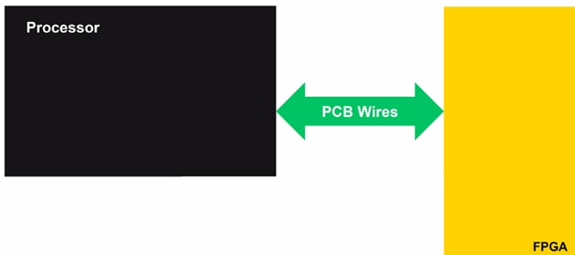
- FPGA Needs central controller and Memory management : Dual Chip Solution needed
- External FPGA and Processor Requires to be connected Externally
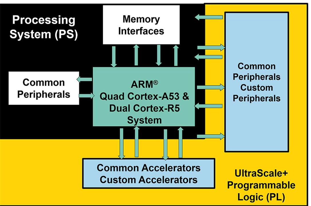
- Solution is to combine FPGA and SoC in Single Chip
- Processing System : ARM Quad core A53 and Dual core R5
- DRAM, Flash, SD for memory interface
- SPI, i2C, UART, Gigabit Ethernet, SATA, PCIe
- PL can be used to provide Custom Peripheral Interface
- Common and Custom accelerator
- 1.5GHz with 13800 DIMPS performance
- Zynq Ultrascale Architecture - From Datasheet
- Optimised and Simplified HW/SW partitioning
- Hw acceleration enables scaling SW performance to address many applications
- Low latency interfacing for efficient co-processor implementation and high throughput data transfers.
- C application can be Run at A53 and R5 Processor
- HDL can Run at PL
- Hw handles heavy data path algorithms
- SW controls and updates the algorithms
- Intensive recurring tasks can be embedded through adaptive algorithms
Advantage of using an a Soc in system level
- Reduced power reduction
- Reduced latency
Hardware software Codesign Flow
- Processor boots first like an ARM based Soc
- PL Can be left unconfigured while developing the real HW
- PL can be programmed through JTAG
Security Features
- ARM Trust Zone
- PS to PL Data can not be snooked externally
- Encryption and crypto accelerators
- Key Rolling
SW and HW Design Methodology
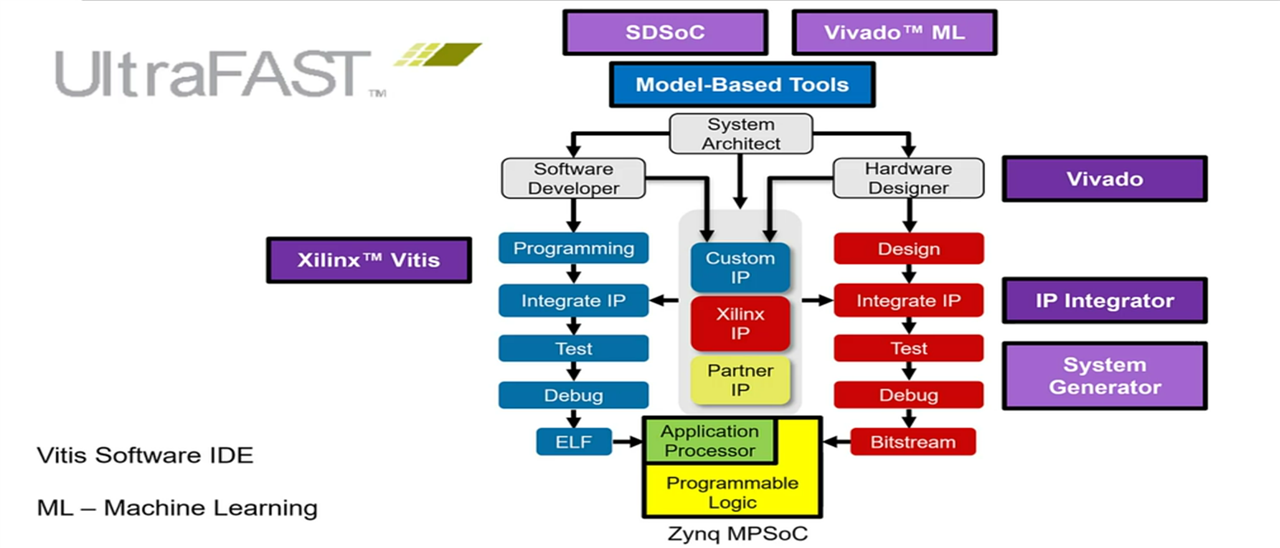
Block Based Design Methodology for Rapid HW Design Flow
LAB 1
| {gallery}Lab 1 |
|---|
|
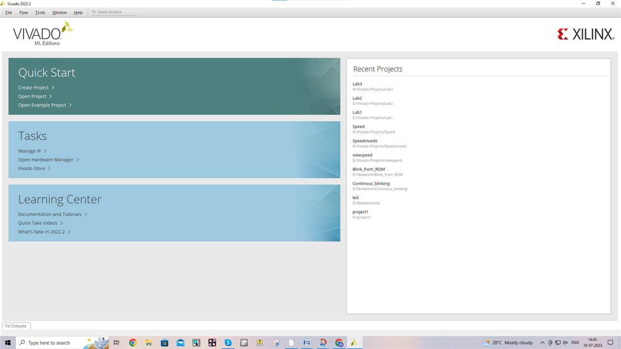
Vivado IDE installed on Windows 10 |
|
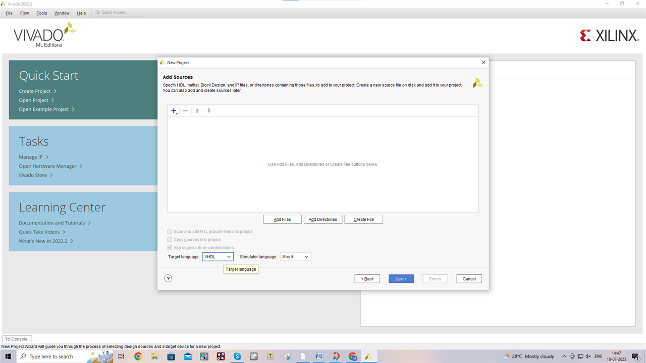
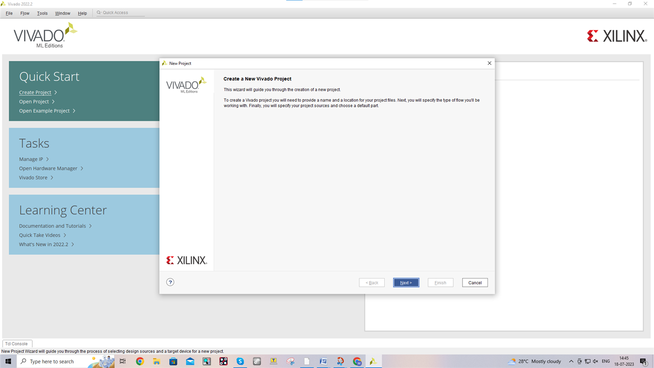
Create a New Project |
|
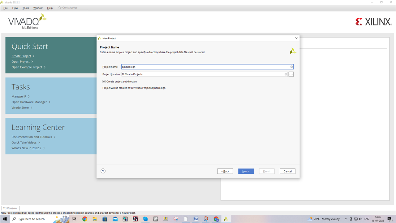
Assign a Project Name |
|
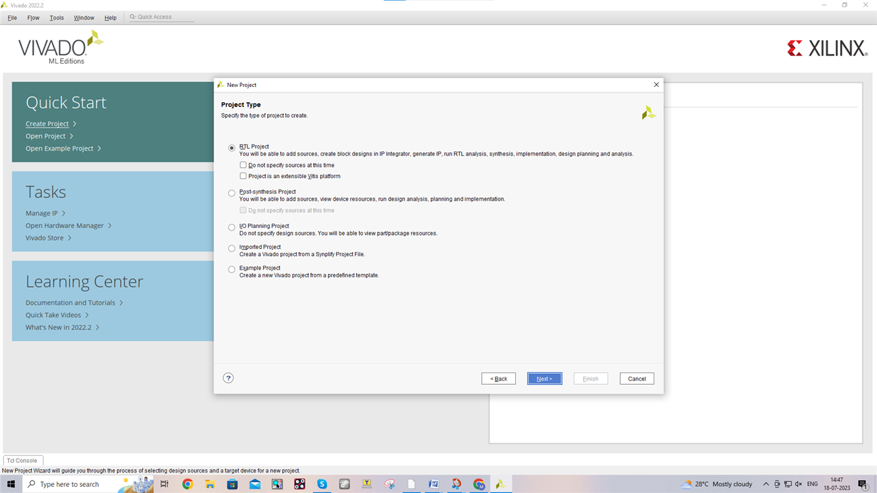
Select RTL Project |
Currently New Project, No need to add any Resource |
|
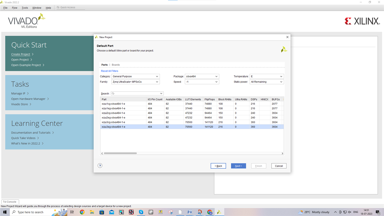
Select the Zynq Ultrascale+ Device used in Ultra96 Board |
|
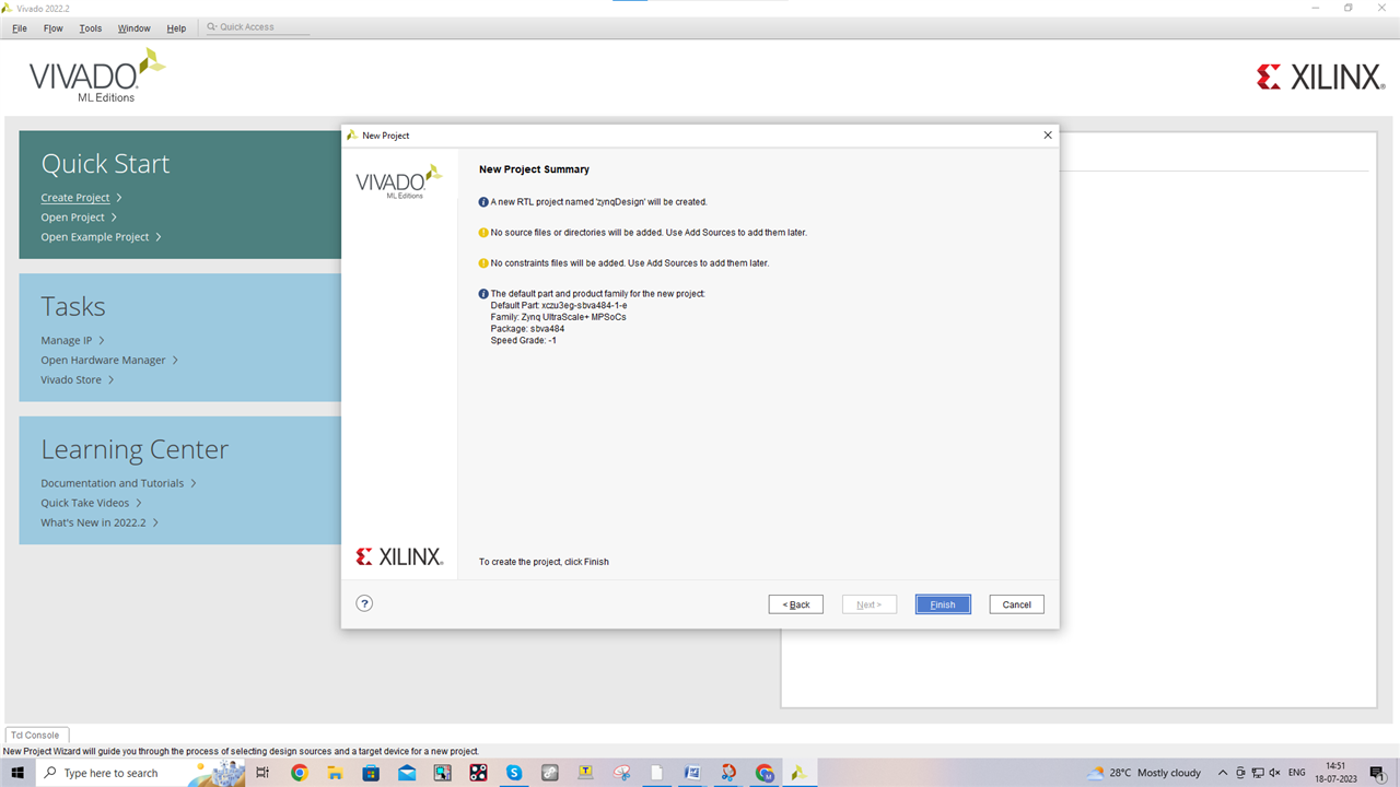
Click Finish |
|
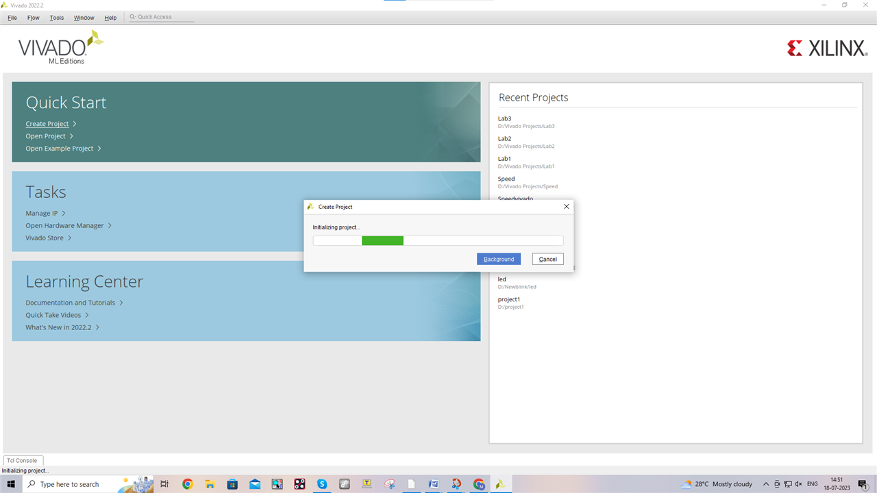
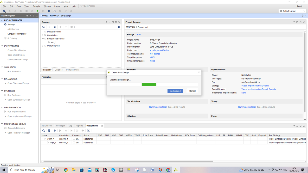
Creating the Project |
|
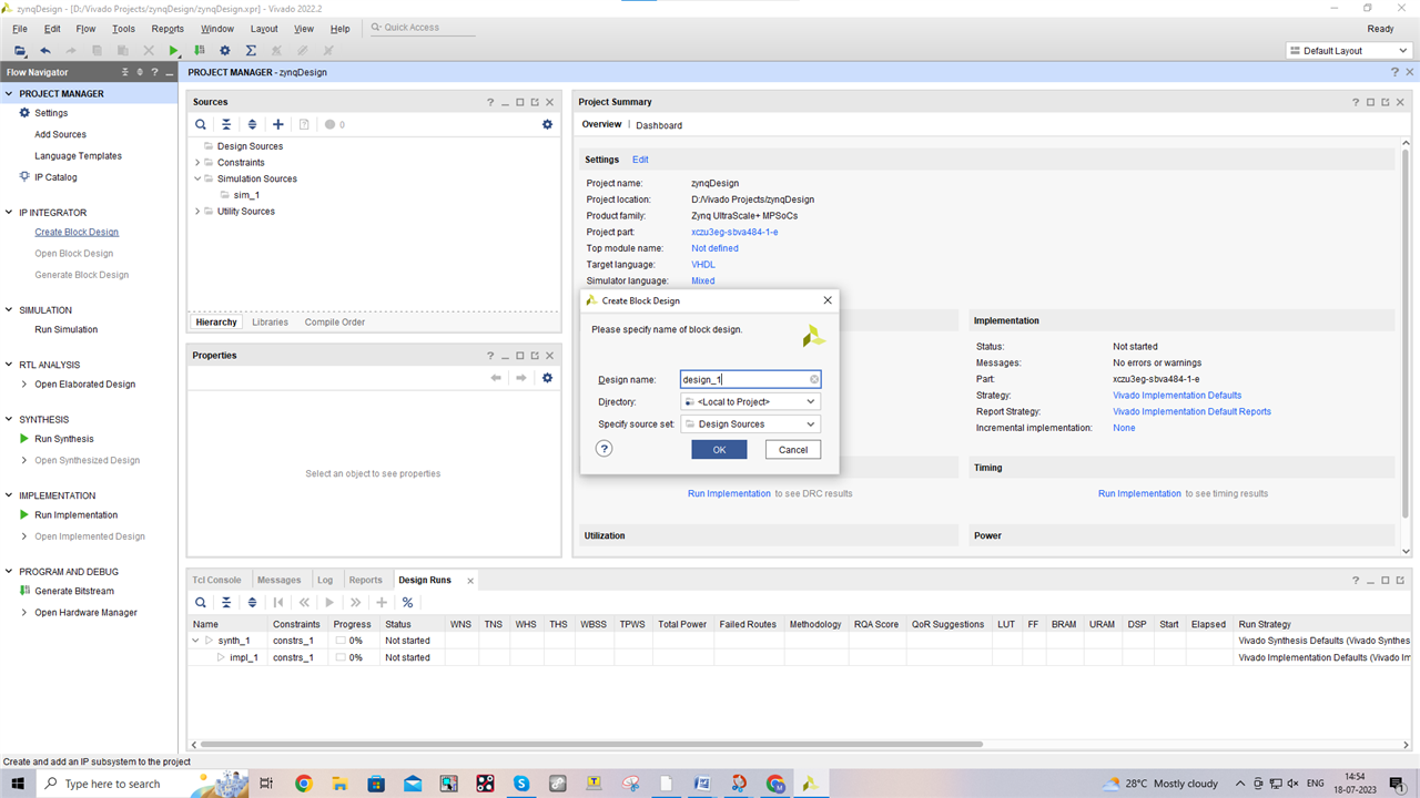
Click on Create Block Design and Give Default name |
|
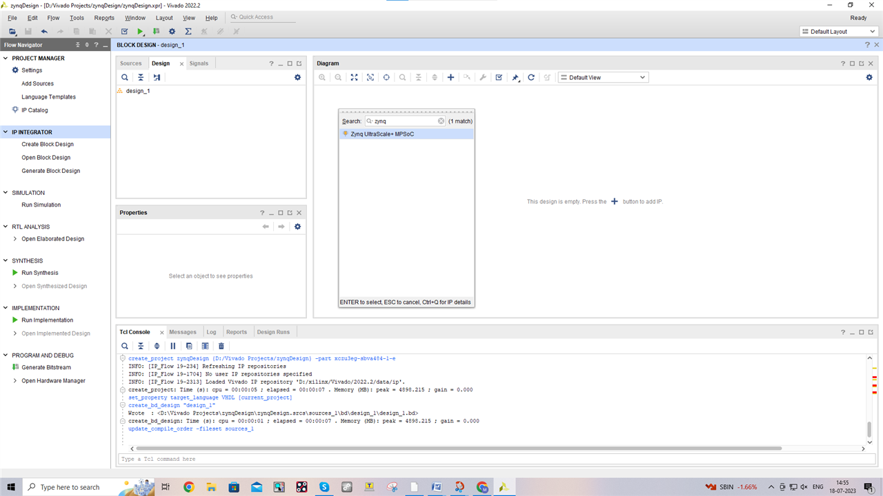
Wait for the tool to load the Block Design windows |
|
Click on + to add Zynq Ultrascale+ IP Block |
|
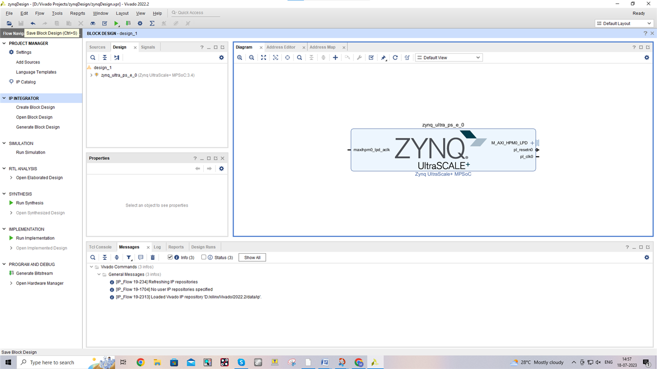
Zynq Ultrascal+ IP block |
|
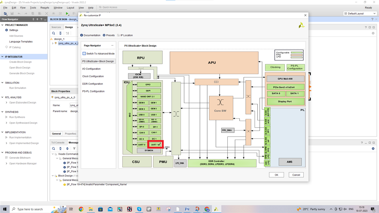
Block Design |
|
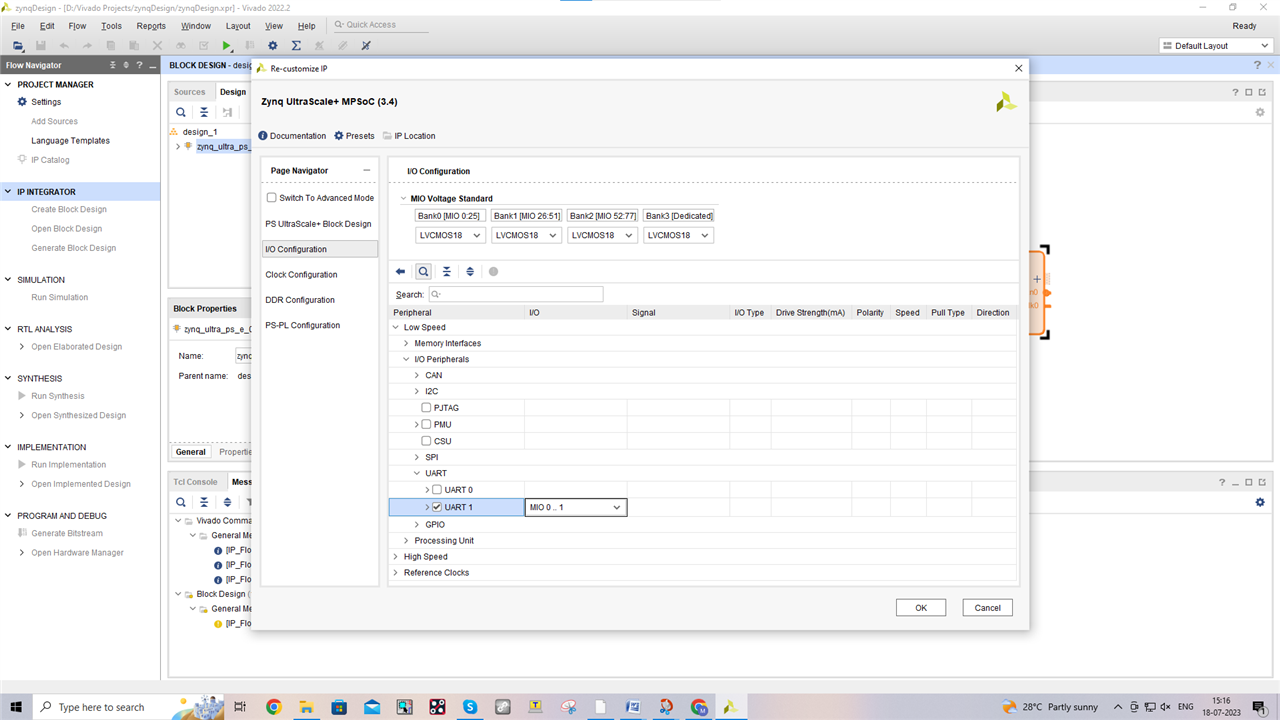
Select UART1 IO configuration: Select the respective MIO Pins to be connected. |
|
UART1 being configured |
|
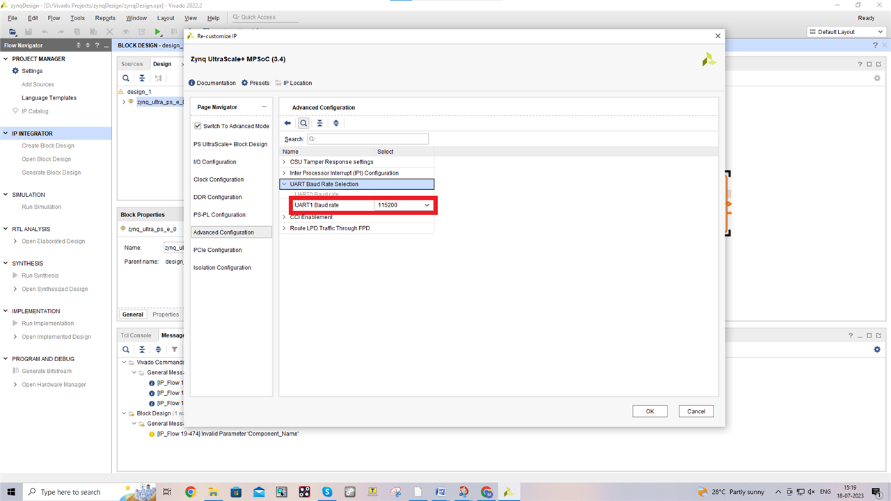
Baud rate can be Hardcoded |
|
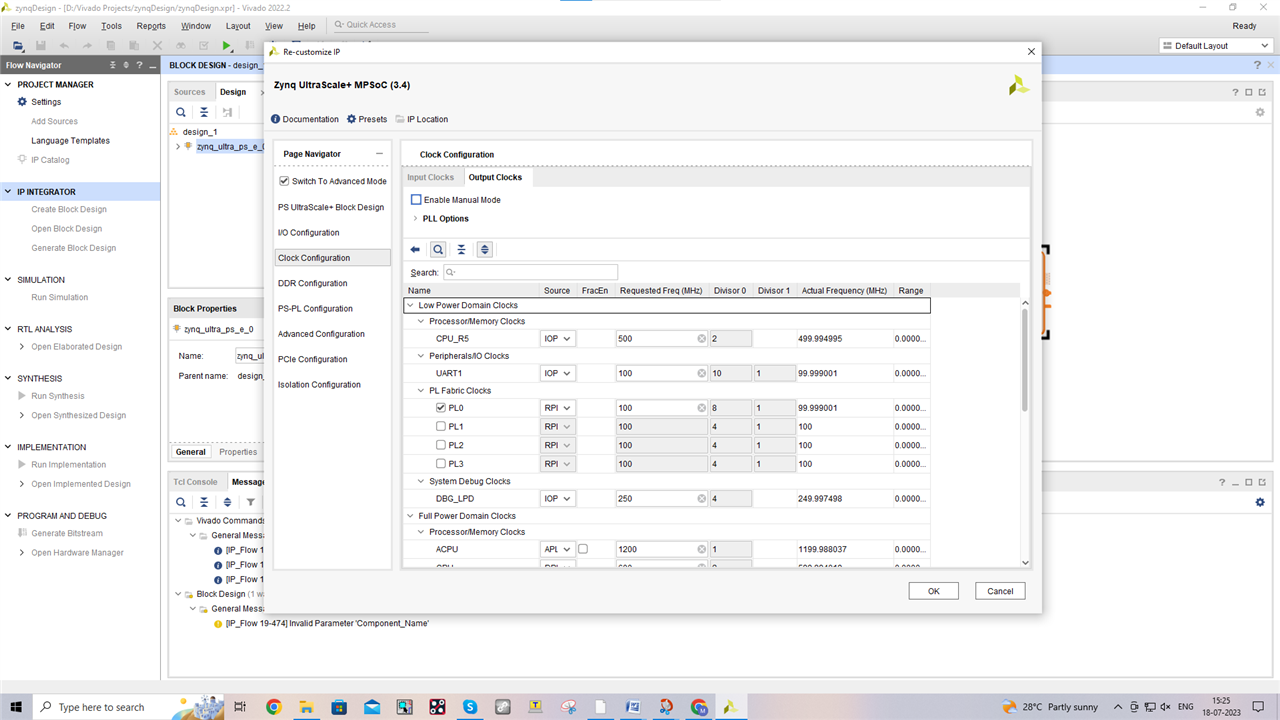
SOC Clocking |
|
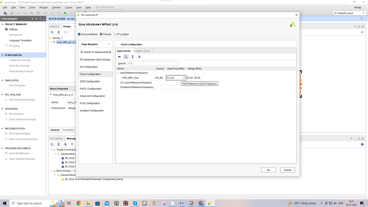
PS REF clocking |
|
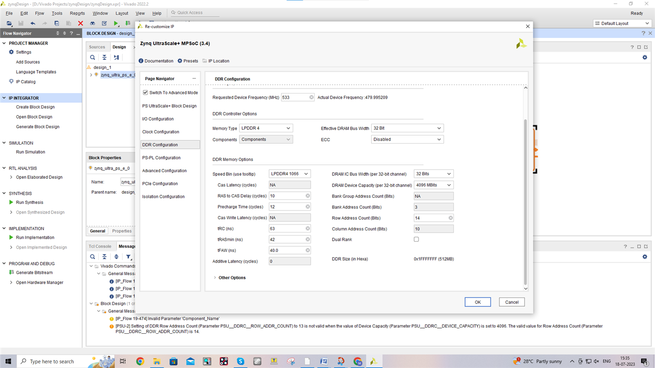
DDR memory Configuration |
|
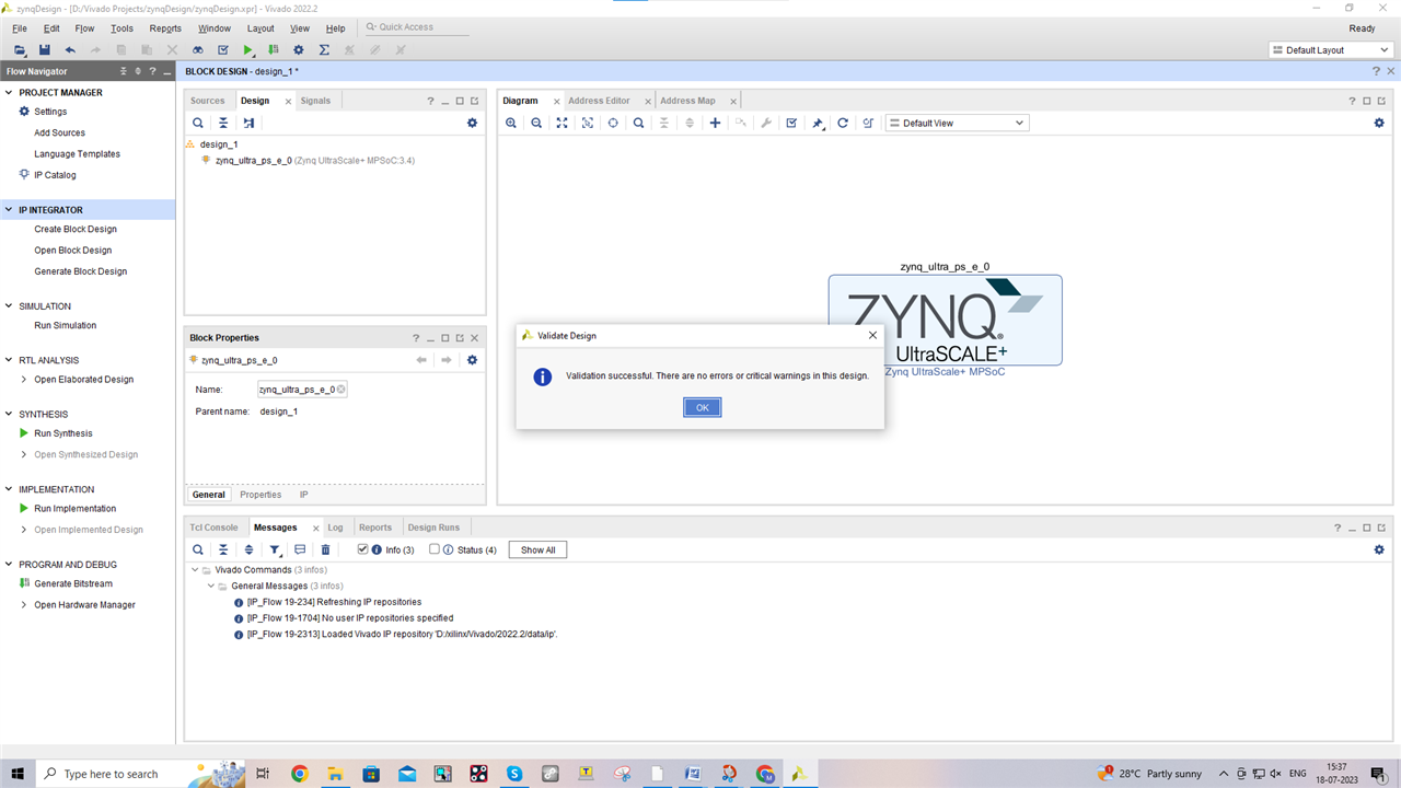
Design validation |
|
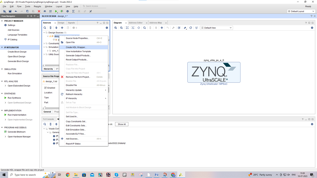
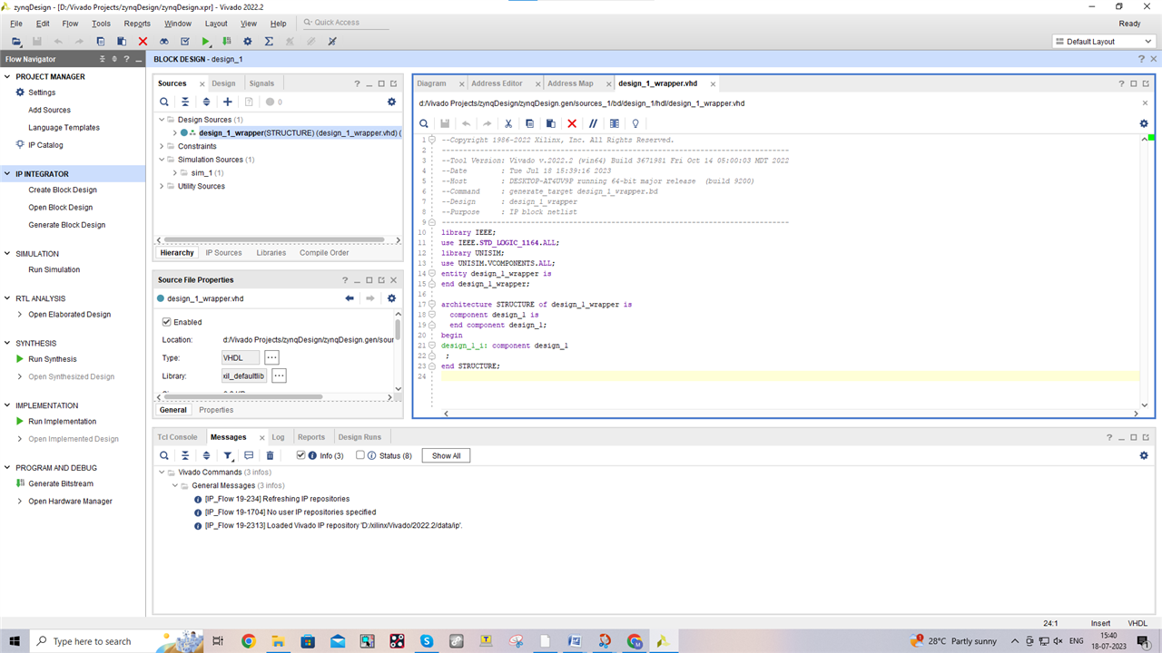
Creating HDL Wrapper : Vivado Create a Basic HDL code : |
|
IP Block Design eases the HDL Files creation : No need to scratch our head to create the base HDL Files |
|
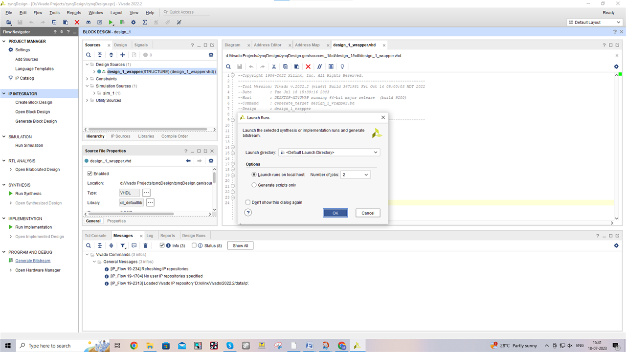
Bits Stream generation |
 REPLACE THIS TEXT WITH YOUR IMAGE
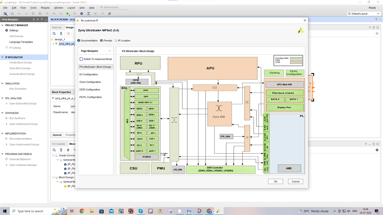
End of Lab1
Lesson 3: Zynq MPSoC Processor Overview:
- Zynq MPSoC PS Blocks
- Quad Core A53, Dual Core R5
- Arm Mali GPU
- Security UNit
- TrustZone
- Encryption
- V/T Monitor
- Platform Unit
- Power & System management
- DDR Controller
- DDR4/3/3L LPDDR4/3 controller
- 256KB OCM with ECC
- High Speed Connectivity
- DP, USB3.0, SATA, PCIE Gen2, PS-GTR
- General IO Connectivity
- Gigabit Ethernet, CAN, UART, SPI/QSPI, NAND, SD-eMMC
- AXI,Clocks and Reset Interfaces
Power Architectures
- 4 Power Domines
- LPD
- FPD
- PLPD
- BPD
- Explanation on A53
- Supports 2.3DMIPS/Mhz and upto 1.5Ghz operation.
- Emploes Harward architecture with 64-bit data and instruction set.
- ARM Cortex-R5 Processor
- Dual Core 600MHz
- 67/2.02/2.45 DIMPS/MHz
- IEC 61508 and IEC26262 - Functional Safety Standards
- Supports Lock Step Cores
- ARMv7-R with HW FPU
- For Real Time applications, redundant core operations
- Cache Coherence : uniformity of Data being stored at Multiple Cache Locations
- Multi Level L1 - Fastest and Limited Size, L2 - Faster - Larger Size
- Layered above the memory
- Snoop Control unit
- Migrate modified Data in one L1 Cache to another
- Process ACP(accelerator coherency port) Transactions
- Cache coherent interconnect
- Connects APU, TCU, IOs, Core Switch
- A central element connects multiple units
- APU transactions pass though CCI on ACE - AXI Coherency Extensions
- Full and IO coherency levels
ARM Cortex-R5 Processor
-
- DDR3, 3L, 4, LPDDR3 and LPDDR4 Modes : Up to 32G Memory capcity
- Up to 2400 Mb/s or MT/s
- 32 and 64 Bits configuration with ECC will be additional 8 Bit
- 5 AXI ports at 128 Bits and 1 at 64 Bits
- Zynq MPSoC PS PL interfaces - 12 Independent Ports
- ACP 128/64 bit ps Slave
- X4 high Performance 32/64/128bit PS Slave
- X2 High performance Coherent(HPCx) PS Slave
- X1 AXI Extension PS Slave
- X2 high Performance PS Master port for FPD Masters
- X1 high Performance PS Master Port for LDP Master0
- X1 LPD Slave
- Zynq MPSoC Clock Generation Module
- One Primary clock Inputs and 4 Alternative inputs
- Generates clocks for APU, RPU, IOU, DDR
- PS_CLK - 27-66MHz : 33.33 MHz Recommended
- 4 GP Clock outs are generated - Frequency can be set accordingly
- clock Group
- Main clock Groups - Support LDP and FPD
- Secure Clock Groups - Internal 200MHz clock for CSU
- RTC Clock Groups for RTC 32 KHz
- Interface clock groups - Peripheral clocks and PL clocks
LAB2: PS Configuration Part 1 - HelloWorld
Please feel to provide your comments and feedbacks.
The Learning with Element14 Community continues...
Regards
Prashanth Kumar G N
-

vishnu123
-
Cancel
-
Vote Up
0
Vote Down
-
-
Sign in to reply
-
More
-
Cancel
Comment-

vishnu123
-
Cancel
-
Vote Up
0
Vote Down
-
-
Sign in to reply
-
More
-
Cancel
Children