Hardware Training Summary
Zynq MPSoC General connectivity
PS IO : MIO only
- Qual SPI
- NAND
- GEM - Gigabit Ethernet
- USB2.0 through ULPI interface
- GPIO : 0-2 Bank
EMIO/EMIO Possibility
- SD/SDIO/eMMC
- Control Area Network
- I2C
- UART
- SPI
- Trace
- Software Watchdog
- GPIO - EMIO also can be used
only EMIO
- GEM as GMII
- UART modem Signals ( CTS,. RTS, etc)
High Speed PS Peripherals : Configurable GTR Transceiver interfaces
- PCIe Gen2 : to x4
- SATA : to 2 Ports
- Display Port
- USB3.0
Interconnect matrix used to determine connection.
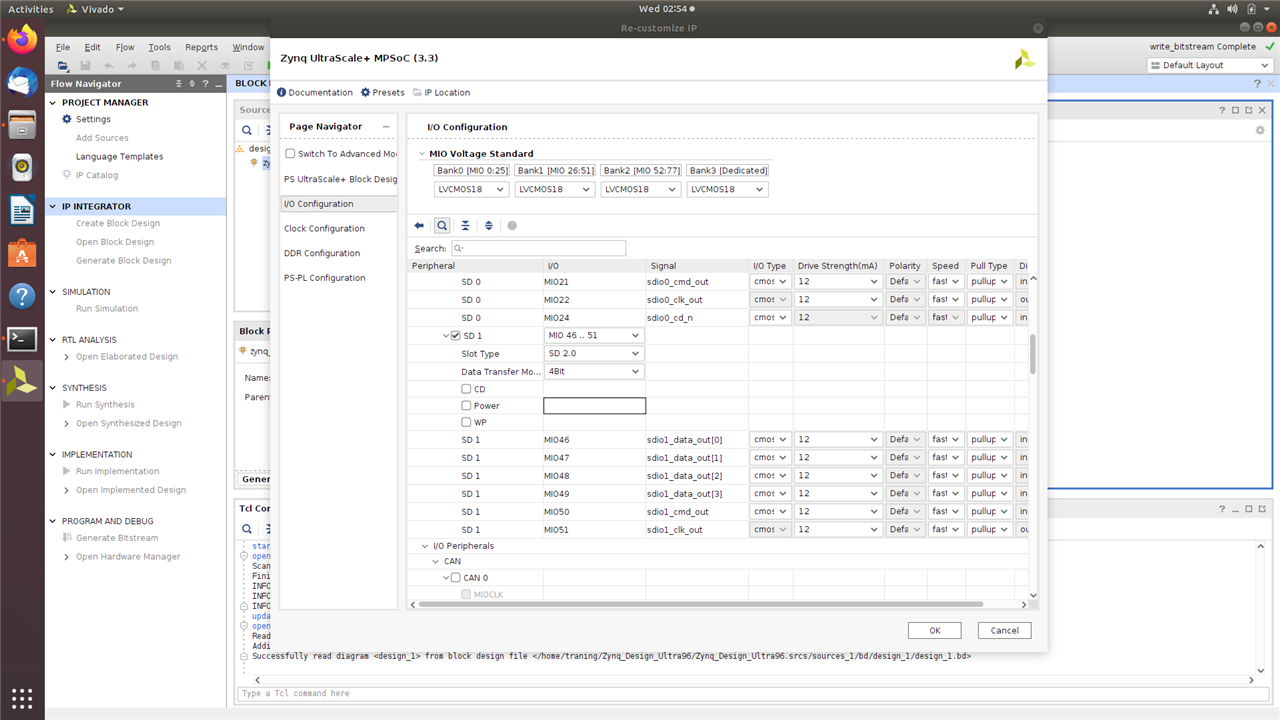
All interfaces are configurable through I/O configuration window.
Assign them to necessary MIO Pins
Zynq MPSoC Memory Map
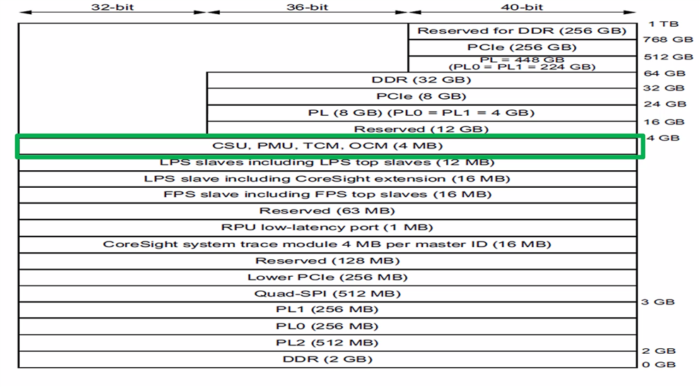
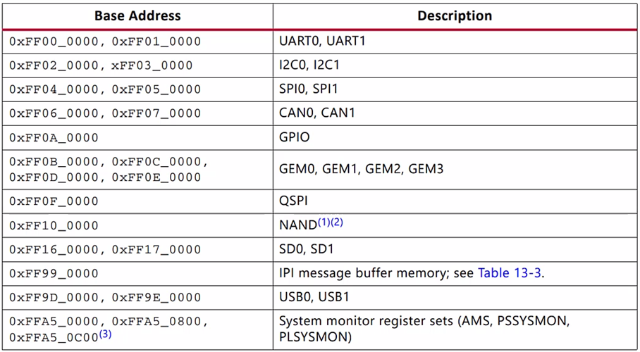
Vivado Assigns address for PL based designs Automatically.
LAB 3 : PS Configuration Part 2 MIO Peripherals
Experiment 1: Enable and Map all PS Peripherals
| {gallery}Lab3 : Experiment 1 |
|---|
|
SD0 and SD1 Interface selection |
|
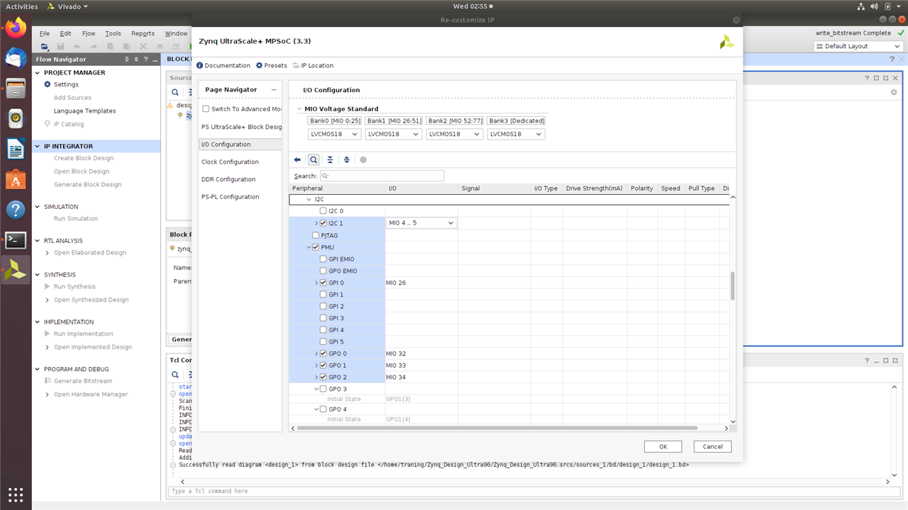
I2C0 and GPI, GPO interface selection |
|
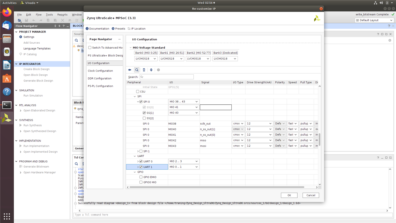
SPI and UART interface Selection |
|
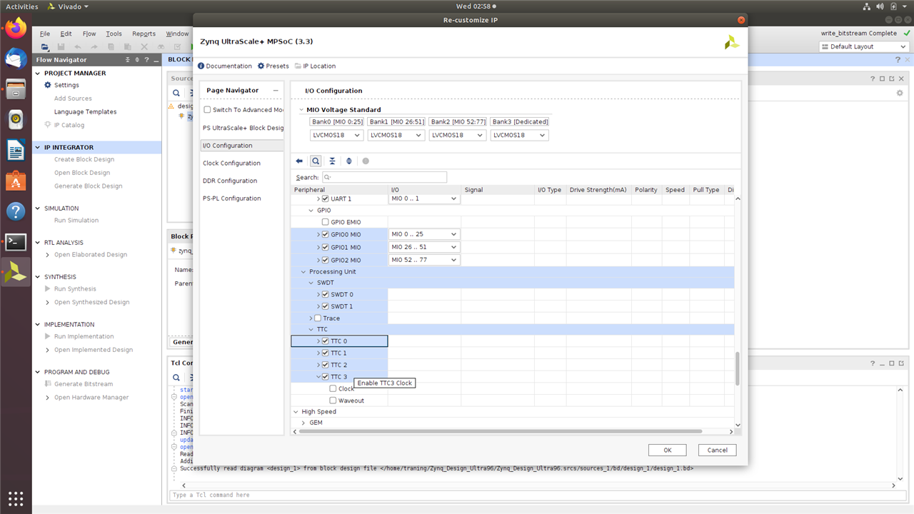
GPIO MIO, SWDT and TTC interfaces |
|
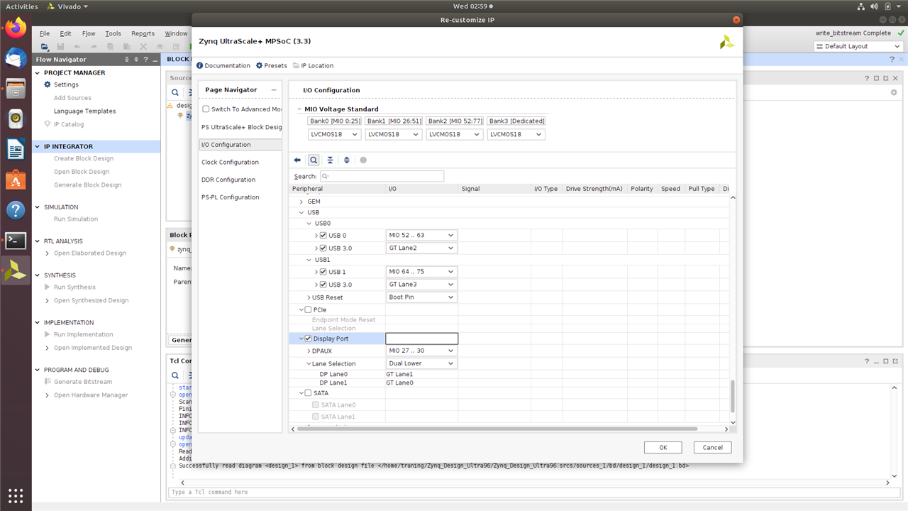
High Speed Port Selection : DP : GTR lanes 0-1, USB 3.0 - GTR Lane 2, USB3.0 GTR Lane 3 |
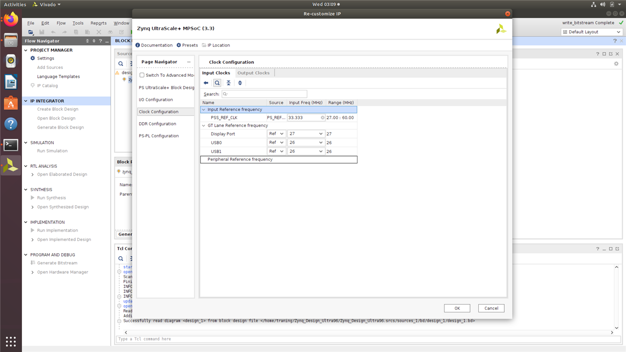
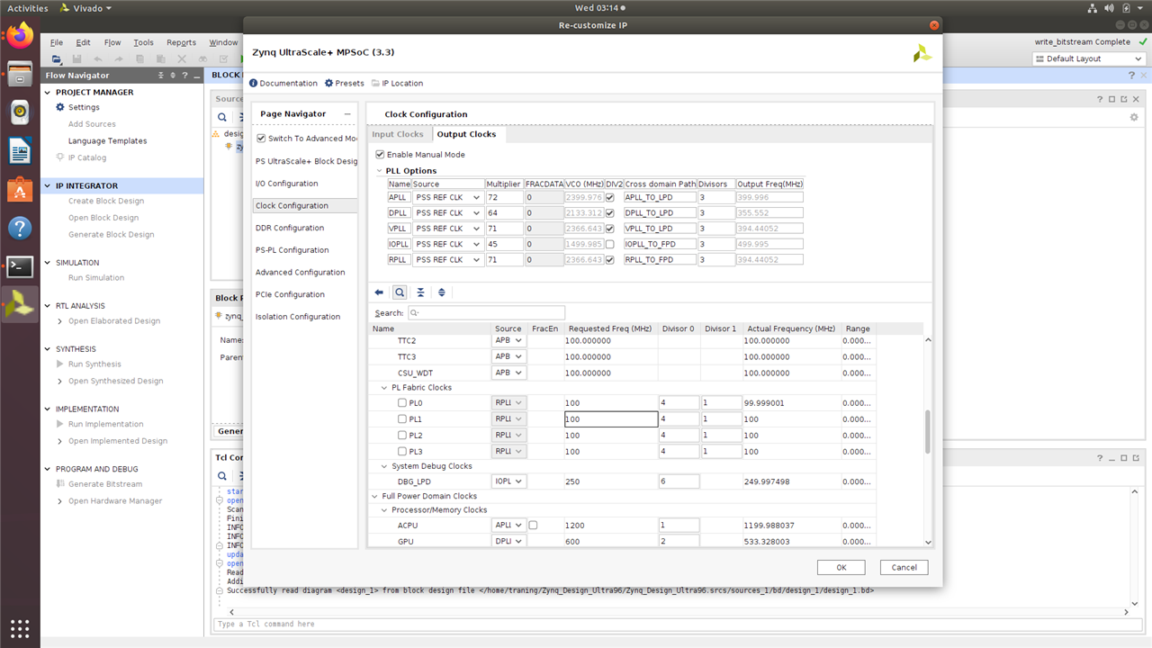
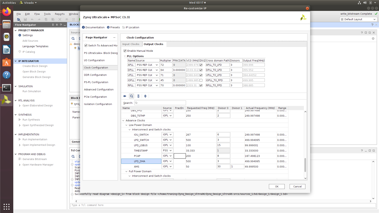
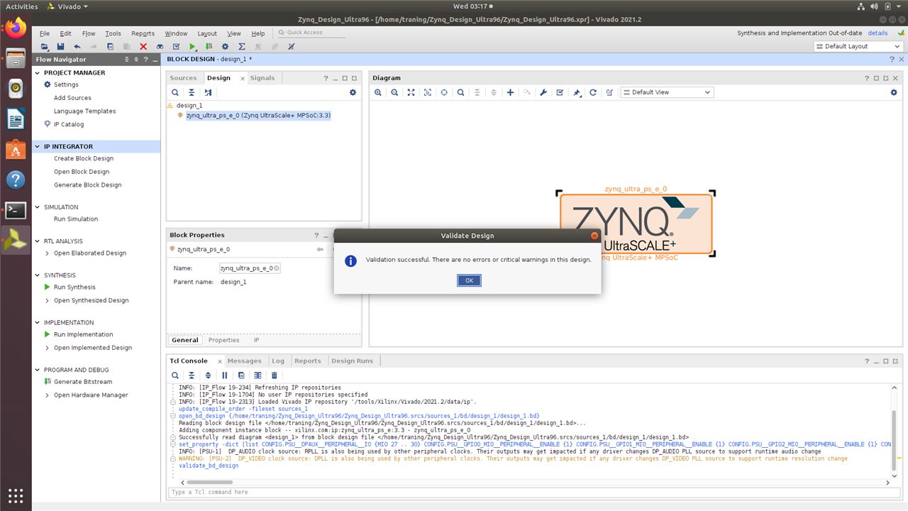
Experiment 2: Set the PS Clocks
| {gallery}Set the Clocks |
|---|
|
Set the Input Clocks |
|
Set the out Put clock : PLL modes |
|
PLL Settings |
|
Validate the Block Design |
|
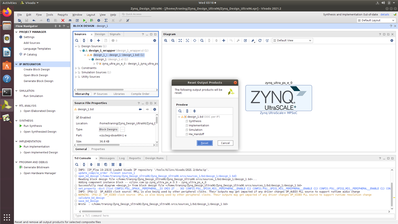
Reset the output parameters |
|
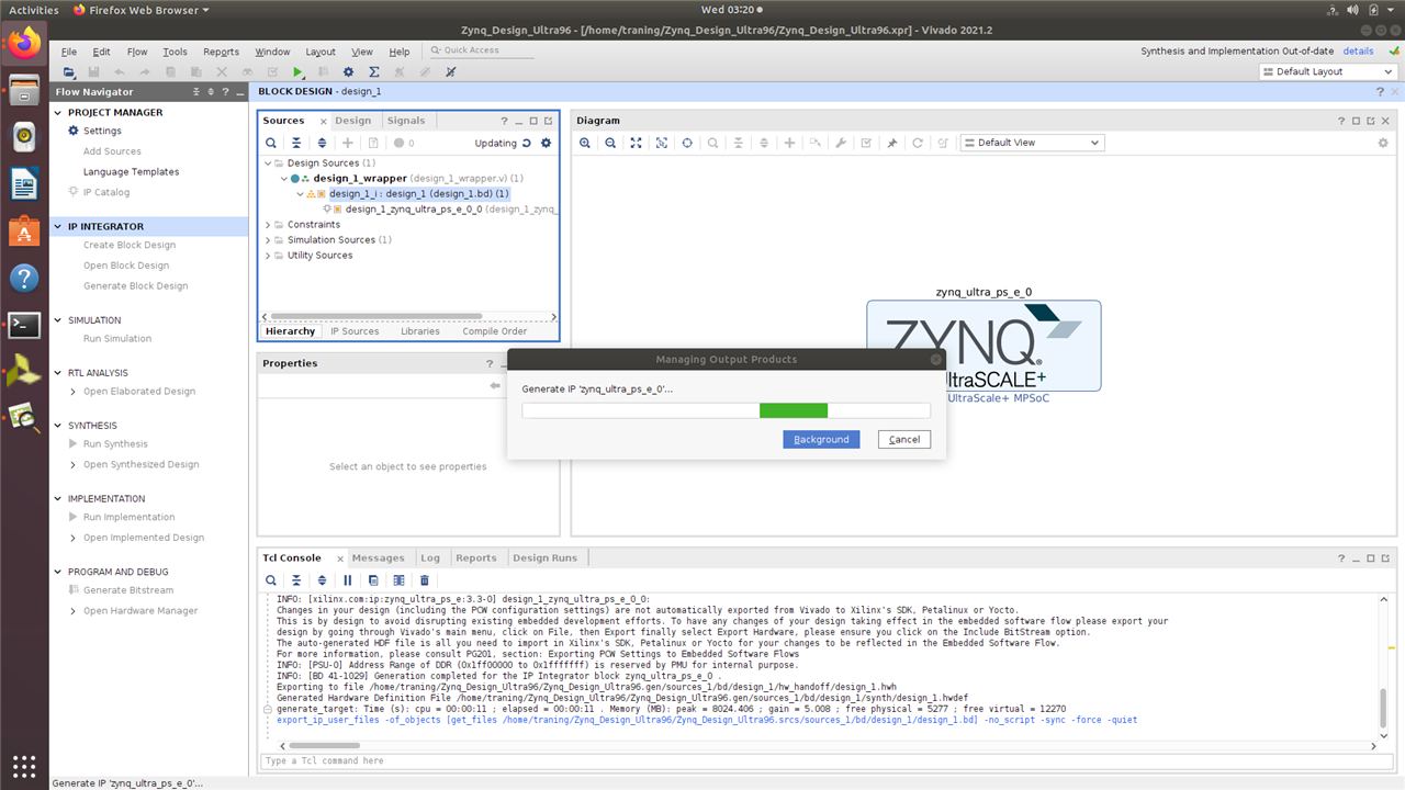
Generation of output Parameters |
|
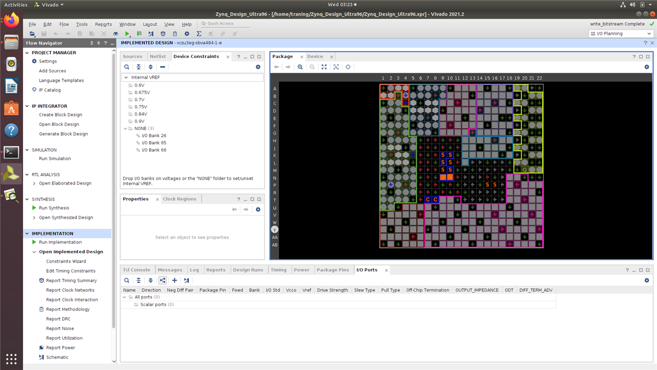
Bistream Generation |
Experiment 3: Create and Run Test Applications
| {gallery}Memory Application |
|---|
|
Opening the Platform Project |
|
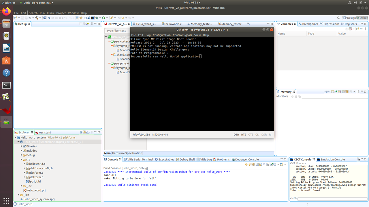
Hello World Application |
|
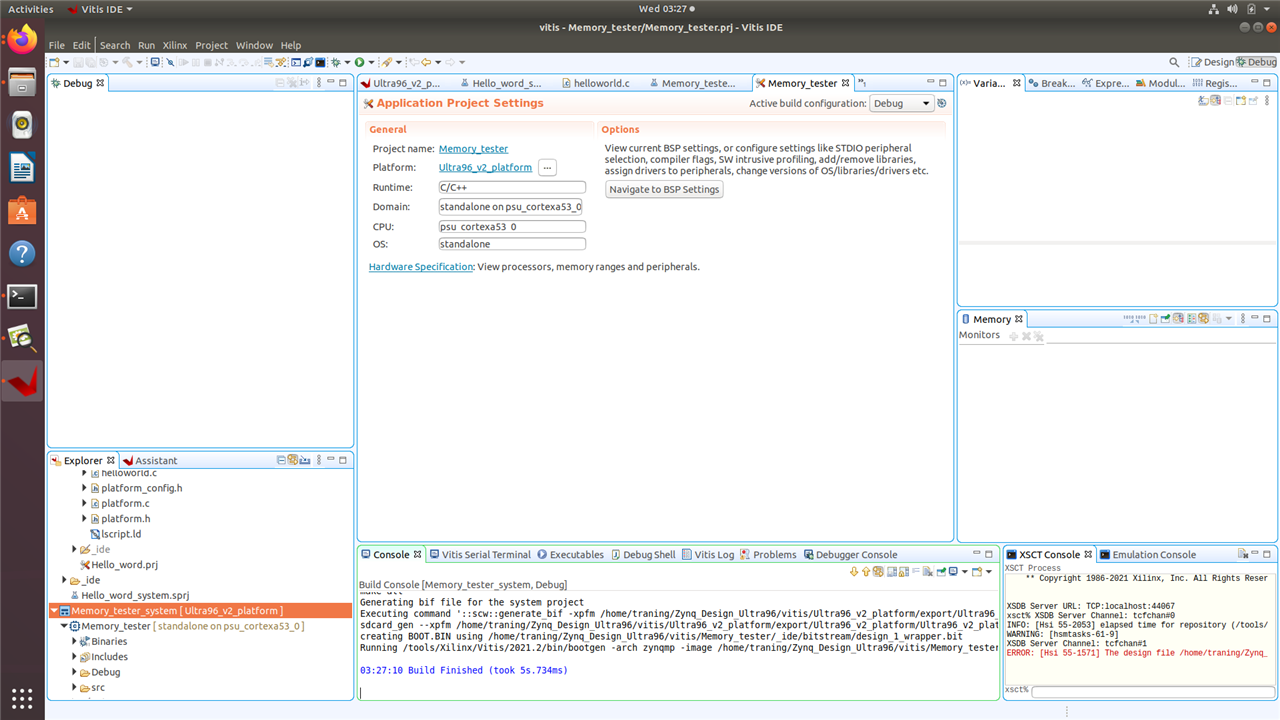
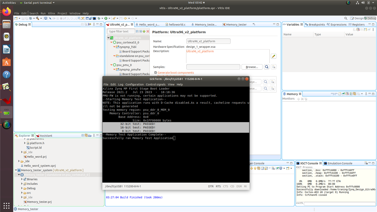
Memory Application Test Passed |
Peripheral test
What is TCL ?
- Tool Command Language
- unite command Languages in all sort of EDAs
- TCL is Open Source !!!
- Download & Install Tcl | ActiveState : TCL Webpage
General instruction to TCL
- For Rapid Prototyping
- Scriptiong Application
- Run TCL Commands for any automated process
- Walk through TCL Commands
- TCL can be used to create a Block Design
LAB4 : Using TCL in Vivado Embedded Designs
| {gallery}TCL |
|---|
|
TCL Script |
|
TCL Script -2 |
Lesson 6: Merging the Processing Subsystem (PS) and Programmable Logic (PL)
AXI Ports
| AXI Port Types | Qty |
| Full Power Master Domine Ports | 2 |
| Low Power Domine Master part | 1 |
| Low Power Domine Slave part | 1 |
| High Perfomance Coherent Slave ports | 2 |
| High Performance Slave Ports | 4 |
| Accelerator Coherency Porst ACP | 1 |
| Accelerator Coherency Extension Port | 1 |
| Total | 12 |
- AXI Types: Master and Slave modes only
- Master to master cannot be connected: only unlike Ports can be connected: Master to slave
- Full duplex communication from Master to Slave AXI Bus
- Five AXI Channels
- Read Address
- Read Data
- Write address.
- Write data
- Write Response
- Up to 16 Master and 16 Slaves
- 32~256 Bit data Width
- Dedicated oqn clock Domine for master and Slave
AXI Smart interconnect
- 16 Master -Salve
- 32~1024 Data bits
- AXI protocol compliant
- only Round Robin Arbitration
AMBA BUS : Advanced Microcontroller BUS architecture
AXI Follows Handshakes READY/VALID
AXI4-Lite
- Lite weight
- Design tradeoffs- No burst, No ID, 32/64 Bits only
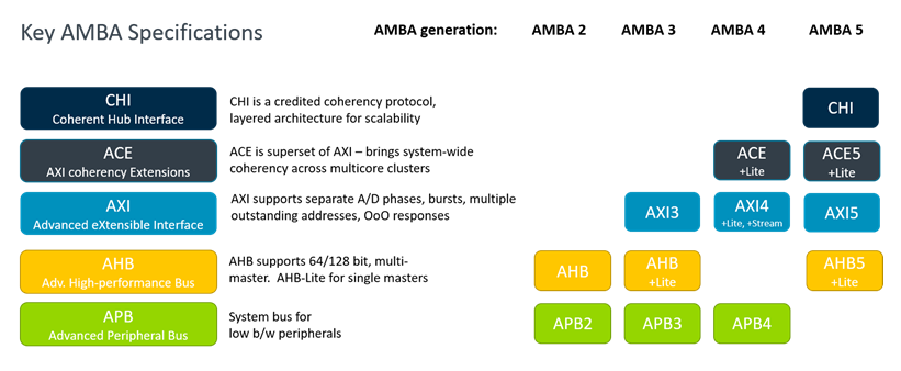
Source : https://semiwiki.com/wp-content/uploads/2020/01/AMBA-history.png
AXI Stream

- FPD/LPD supports 32/64/128 Bit Data bus
- LPD Burt Length is limited to 16 Bits only
- LPD enables Direct access to PL!!! - Like Block RAM and DDR
High performance Slave AXI
- High bandwidth Master to Slave Data
- Access to Memories like DDR, OCM, TCM
- x4 128/64/32 Bit Configuration
- Smooth Long Latency event
- Low latency path for DDR, OCM, TCM
More info available on Zynq Ultrascale+ technicial Reference Manual : Zynq UltraScale+ Device Technical Reference Manual (xilinx.com)
LAB 5 : Adding a PL Peripheral
https://youtu.be/yCUj-xQ5exI
| {gallery}My Gallery Title |
|---|
|
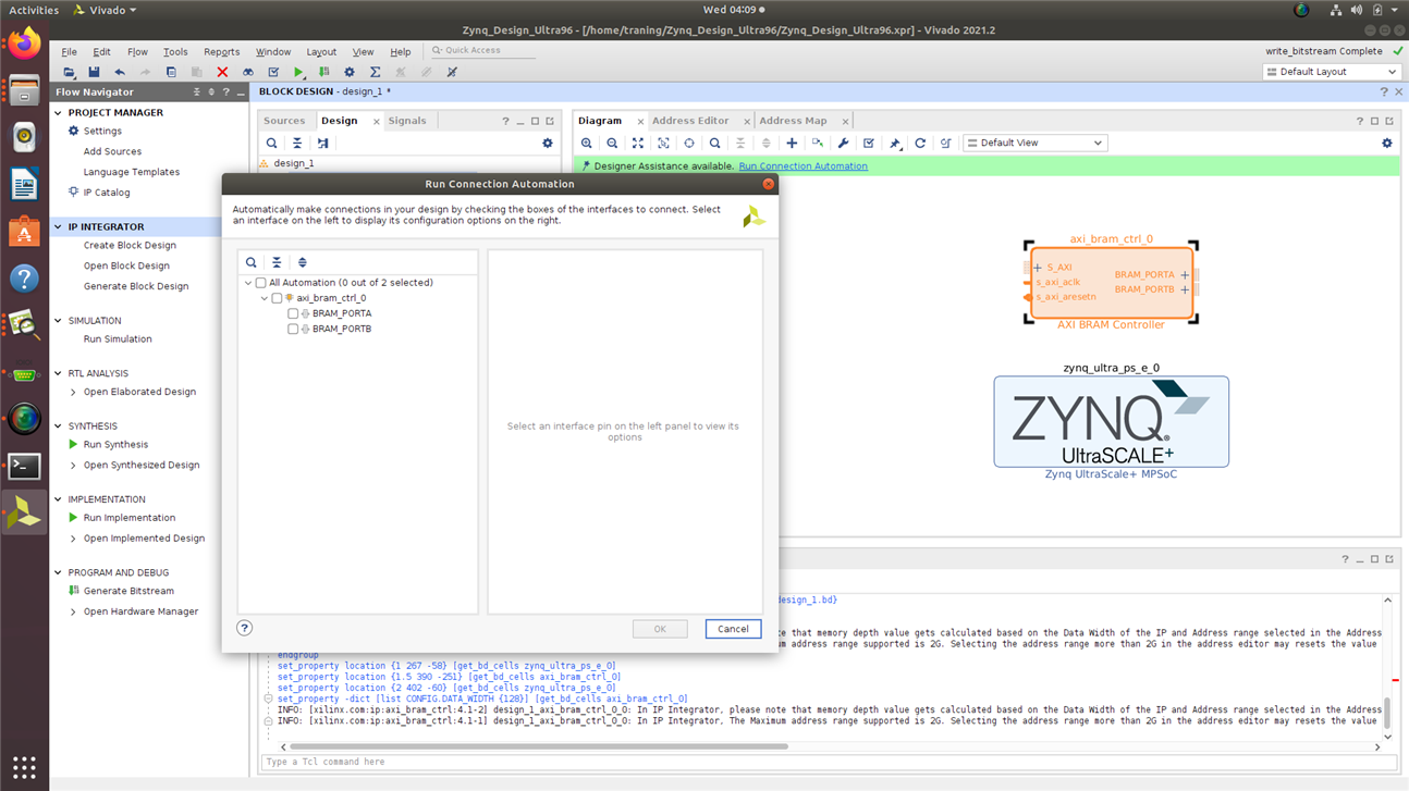
AXI BRAM IP and Connection Automation |
|
Block RAM Generator IP |
|
Zynq Ultrascale+ MP SoC IP : Enabling AXI Master Interface |
|
Connection Automation for AXI Bus |
|
BitStream Generated |
- What is DMA : Direct Memory Access : IOs can access memory directly without CPU involving.
- DMA is the effective way to connect between PS and PL
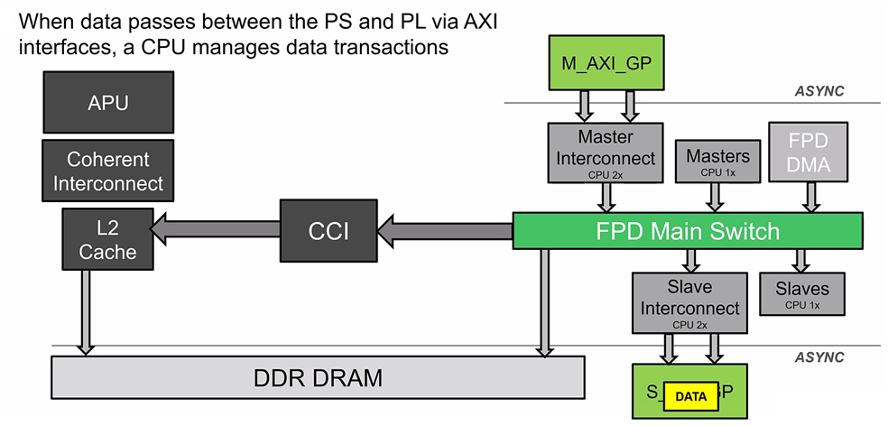
Data Path
- Data from Slave AXI to Slave Interconnect though FPD Main Switch
- Passs though CCI to L2 cache
- from L2 to DDDR DRAM
- FPD and LPD move data between DDR, OCM and Slave PL Peripherals
Additional DMA Controllers included in below peripherals
- PCIe Gen2
- SATA
- Display Port
- Gigabit Ethernet
- USB3.0/2.0
- SD/SDIO/eMMC
- QSPI
Lab 6 Improving Data flow between PL and PS utilizing PS DMA
| {gallery}Lab 6 |
|---|
|
Adding DMA Application |
|
BRAM to DRAM Application Stuck |
|
DRAM to DRAM is passing |
- IP Packers includes
- Source Files
- Simulation Models
- Example Design
- Documentation
- Test bench
- Wizard in Vivado to create an IP!!!
- IP Package creates HDL Source
LAB 7 : Add Custom PL Peripheral
| {gallery}Creating the IP |
|---|
|
Creating the IP |
|
Creating the AXI Pheripheral |
Adding AXI |
IP Created available in catalogue |
Lesson 9: Vivado's Hardware Manager
FPGA Design is an iterative Process.
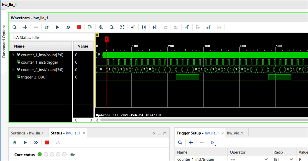
ILA : Integrated Logic Analyzer
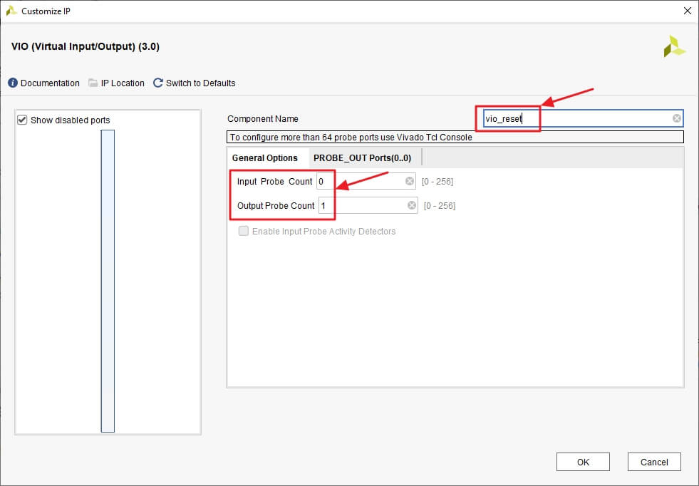
VIO 3.0 : Vivaldo native Virtual input and Output
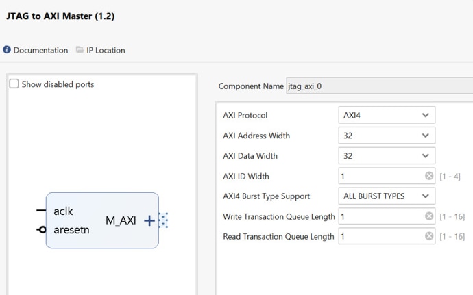
JTAG to AXI 1.2
Lesson 10: Tcl Scripting and Next Steps
- Allow for easy share of Project
- TCL build projects in minutes
the Learning with ELement14 will continues..
Feel free to Share your thoughts.
Regards
Prashanth Kumar G N

-

Murulidharlm
-
Cancel
-
Vote Up
0
Vote Down
-
-
Sign in to reply
-
More
-
Cancel
Comment-

Murulidharlm
-
Cancel
-
Vote Up
0
Vote Down
-
-
Sign in to reply
-
More
-
Cancel
Children