


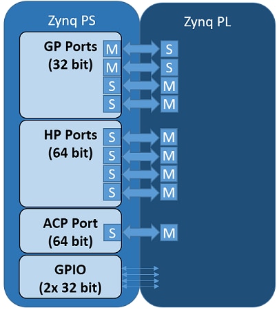
Xilinx ZYNQ-7000 AP SoC consists of a Programmable Logic (PL)(FPGA) and Processing Subsystem(PS) (ARM Cortex-A9). The communication logic/interface between the PL and PS is an essential component of ZYNQ Architecture for data transfer. The AXI Interconnect acts as an important communication link between PL & PS for bi-directional data transfer, compared to other available options. The PL and PS integration allows a high level of performance and reliability that a multi-chip-based solution can't afford.

ZYNQ SoC devices use several communication interfaces based interconnect techniques, optimized and designed to the particular communication requirements of the functional blocks. The interface of PL and PS includes all the connections accessible to the system designer. The communication logic/interface is part of the functional interface type and AXI interconnect is the preferable interface for data communication between PL and PS.
In this blog, I will design a AND gate in programmable logic (PL) and a NOT gate in the processing system (PS). Together it will form a NAND gate. I will test the NAND gate using two switches and one LED. Led and switches will be connected through the external IOs.
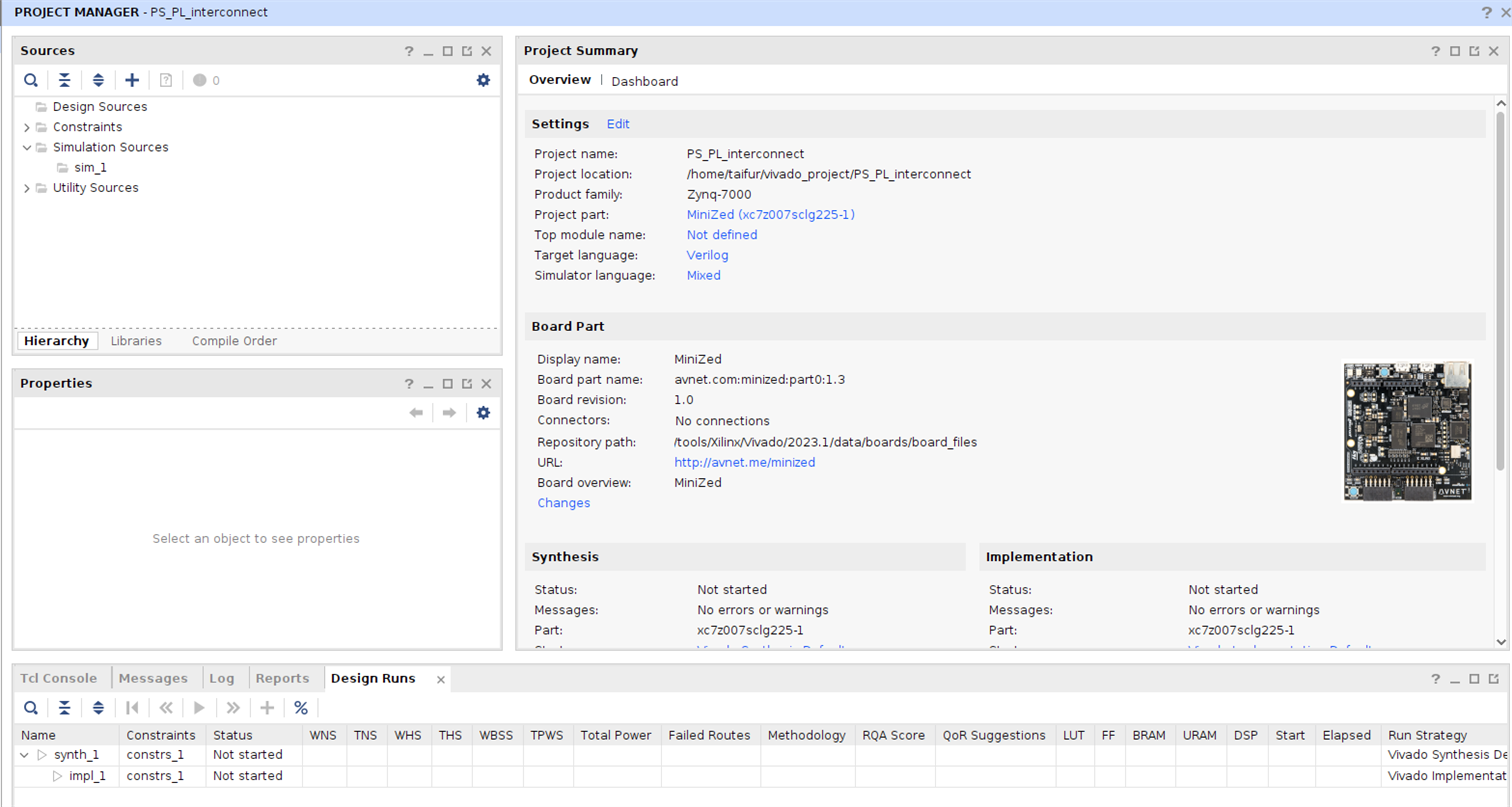
I started by making a new project in Vivado. I named the project as PS_PL_interconnect and I choose MiniZed board as target board. The summary after creating the project is as follows:
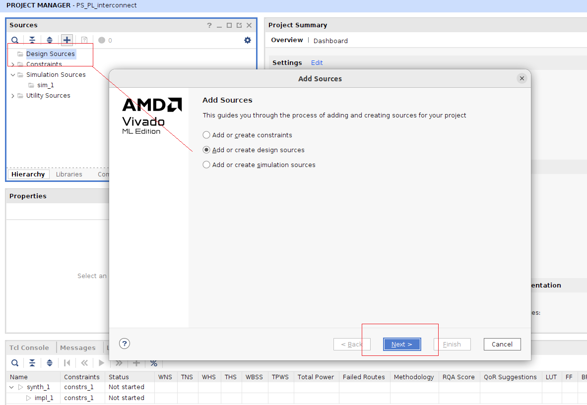
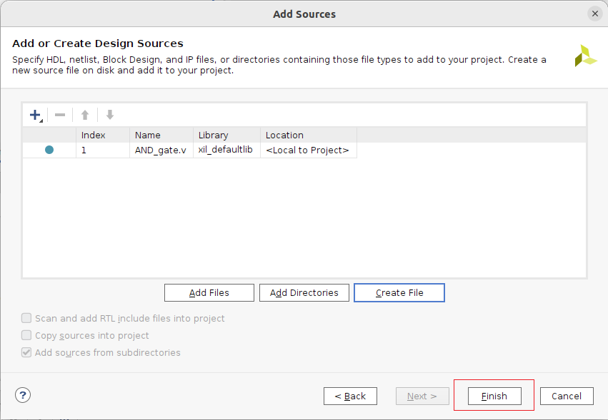
During the creation I did not add any source. So, I am adding a Verilog source here.
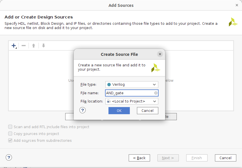
I gave a name of the Verilog source. The name is AND_gate.
After adding the name the source file is created successfully. Now I need to click the Finish button.
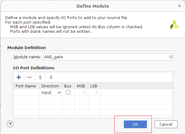
It will ask to add I/O port definition here. It is optional and I just clicked OK.
It will ask for the confirmation. Just click the yes to confirm.
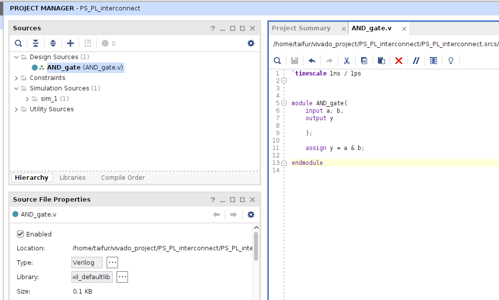
You see a varilog source named AND_gate is added to the source. Double clicking on the source will open the Verilog file. We need to open the file because we will add some code here. For AND gate logic I added the following Verilog code:
`timescale 1ns / 1ps


module AND_gate(
    input a, b,
    output y

    );

    assign y = a & b;

endmodule
After saving the code the next step is to add a constraint file. Right click on Constraints and choose Add Source to add a constraint. The following window will open. Click Next.

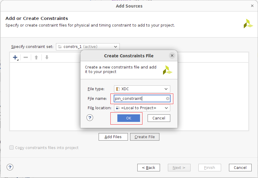
Give a name for the constraint and click OK.
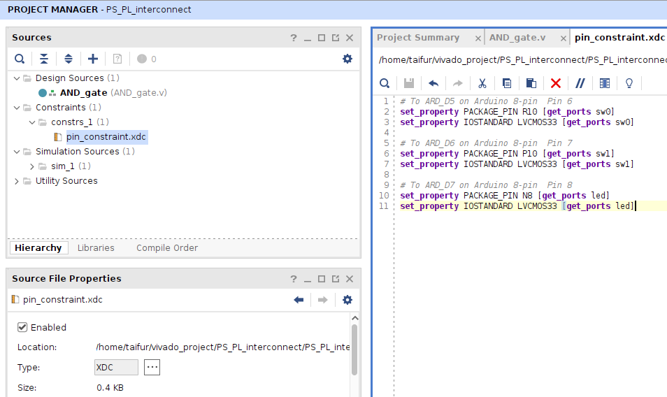
I need two switches for testing the logic as I am added a two input AND gate. I will use two switches for this purpose. I will use Arduino Pin 6 and Arduino Pin 7 for switch. And for led I will use Arduino Pin 8. So, I added the constraints accordingly.
# To ARD_D5 on Arduino 8-pin  Pin 6
set_property PACKAGE_PIN R10 [get_ports sw0]
set_property IOSTANDARD LVCMOS33 [get_ports sw0]

# To ARD_D6 on Arduino 8-pin  Pin 7
set_property PACKAGE_PIN P10 [get_ports sw1]
set_property IOSTANDARD LVCMOS33 [get_ports sw1]

# To ARD_D7 on Arduino 8-pin  Pin 8
set_property PACKAGE_PIN N8 [get_ports led]
set_property IOSTANDARD LVCMOS33 [get_ports led]
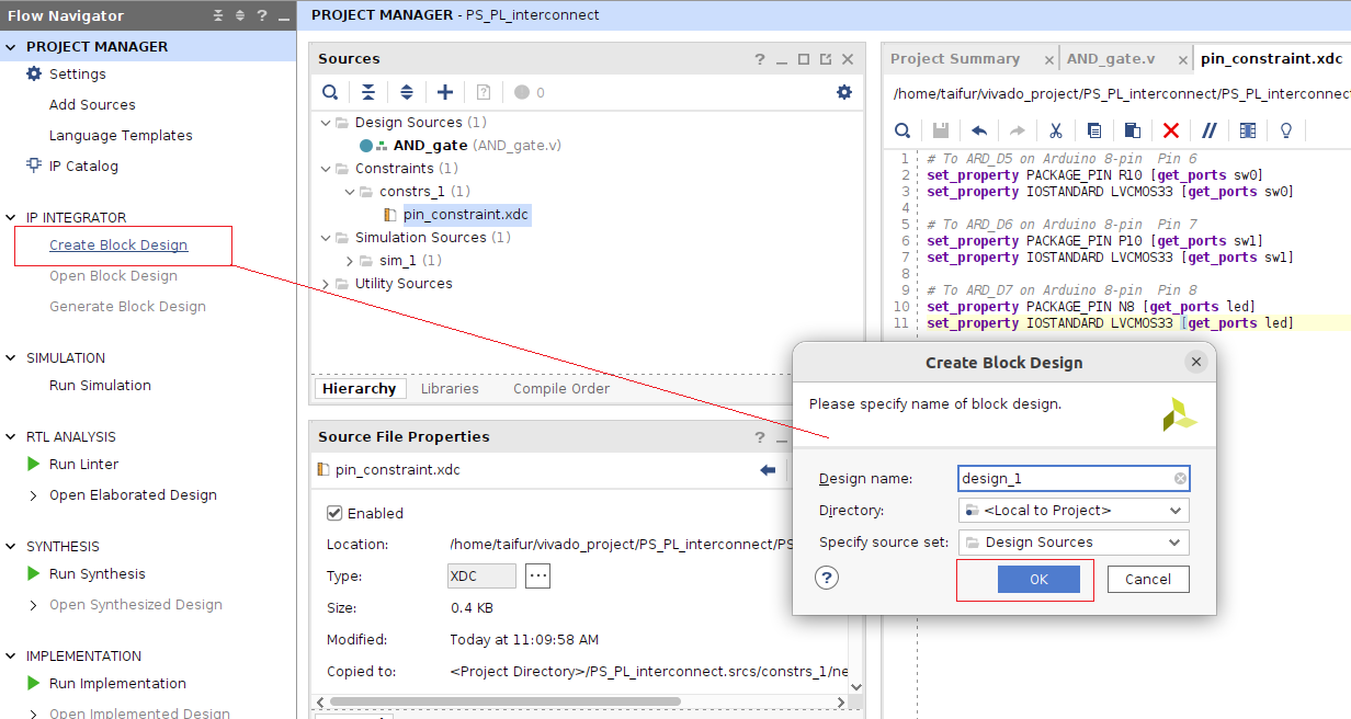
After adding the constraint we will desing our system using Block. So, I created block design by clicking Create Block Design from IP INTEGRATOR from Flow Navigator. I did not change the name. The default name is design_1.
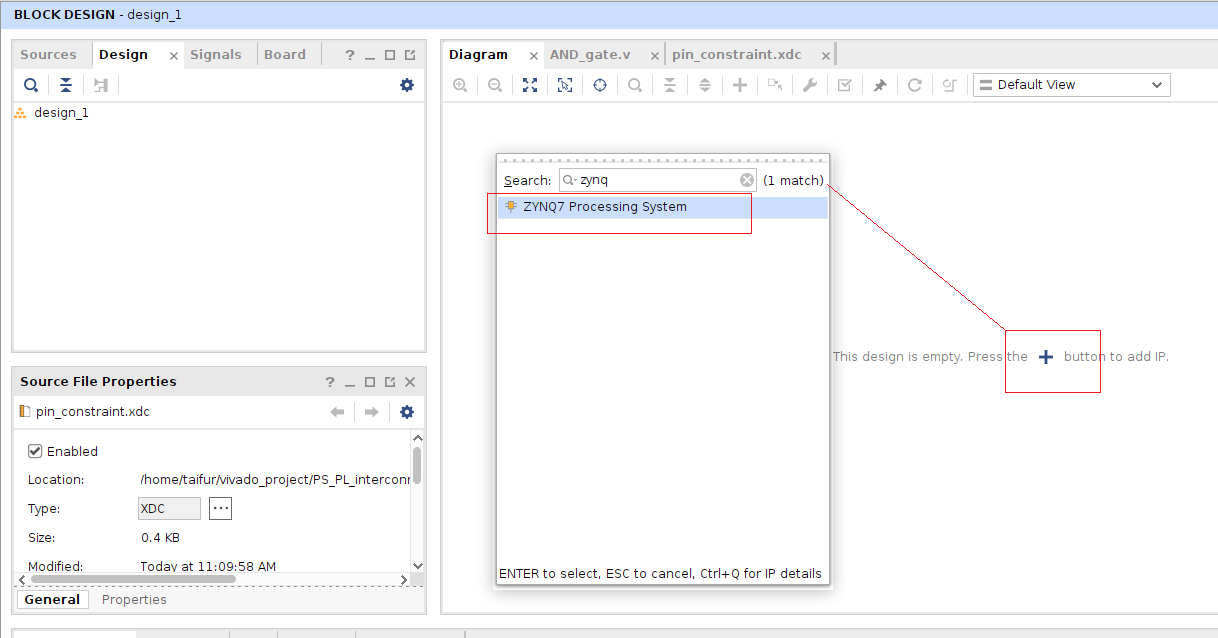
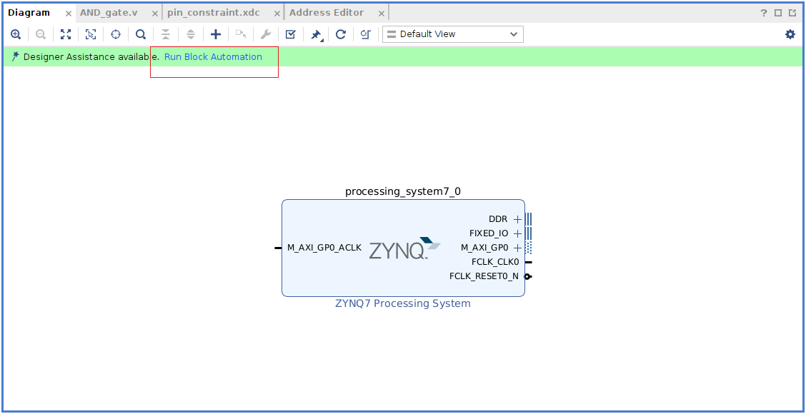
It will open a new window for creating and adding block. I added ZYNQ Processing System first.
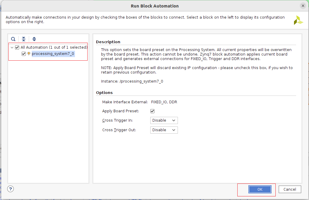
ZYNQ Processing System is successfully added. Click on Run Block Automation for making necessary connection.
Marke all the check boxes and click OK.
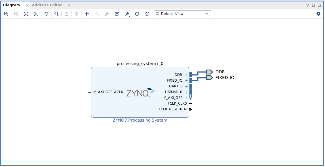
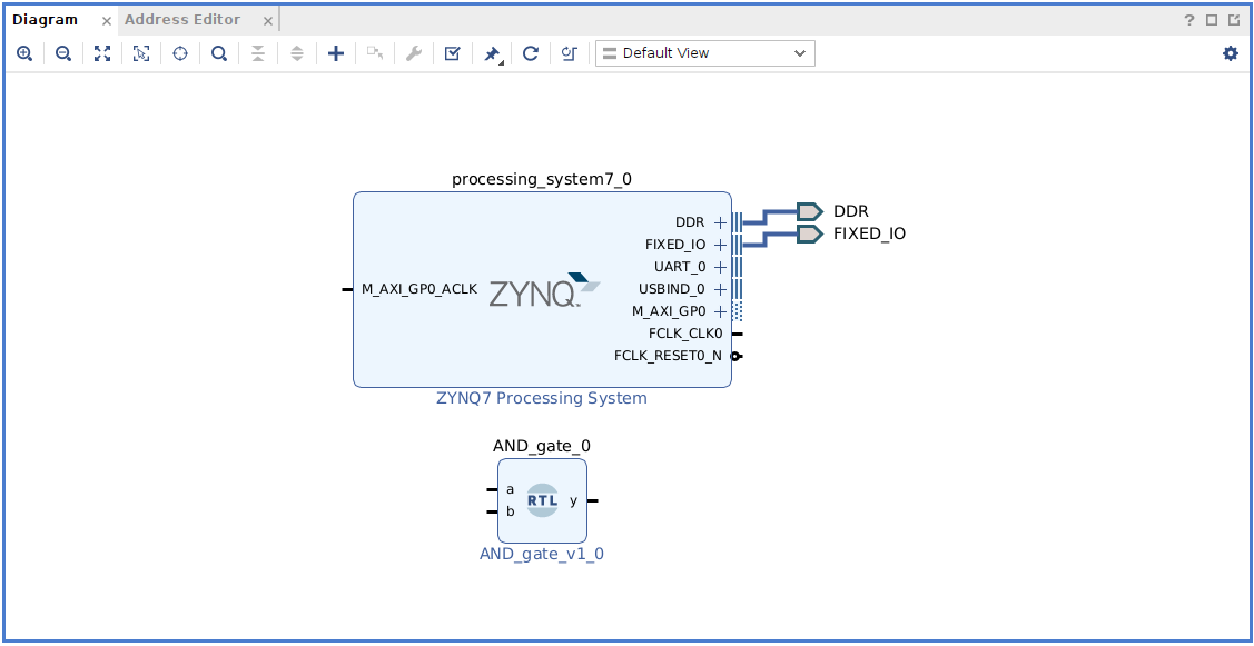
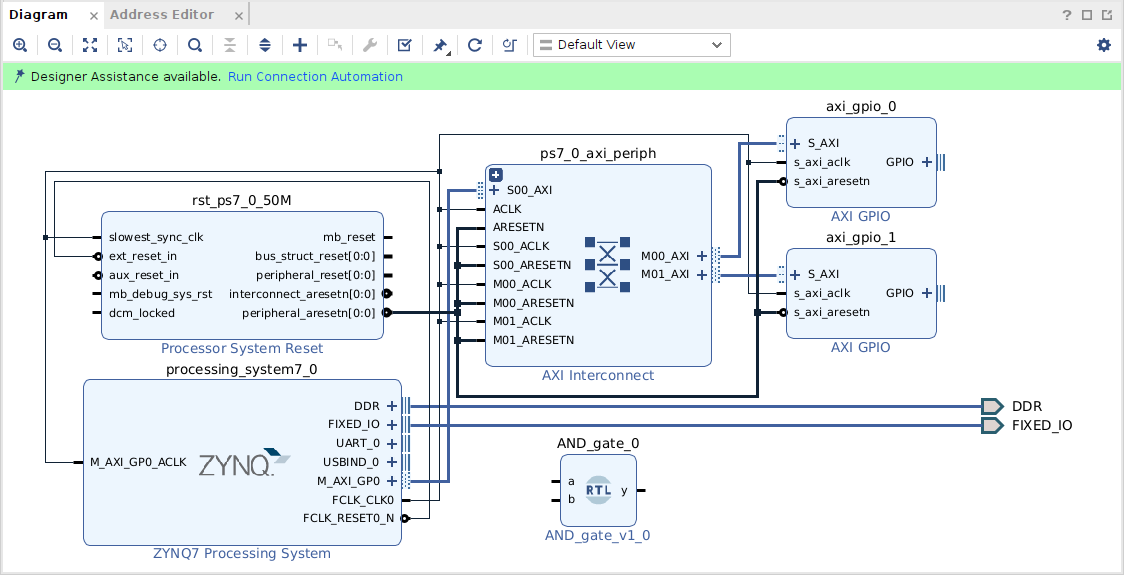
DDR and FIXED_IO is connected after running the block automation.
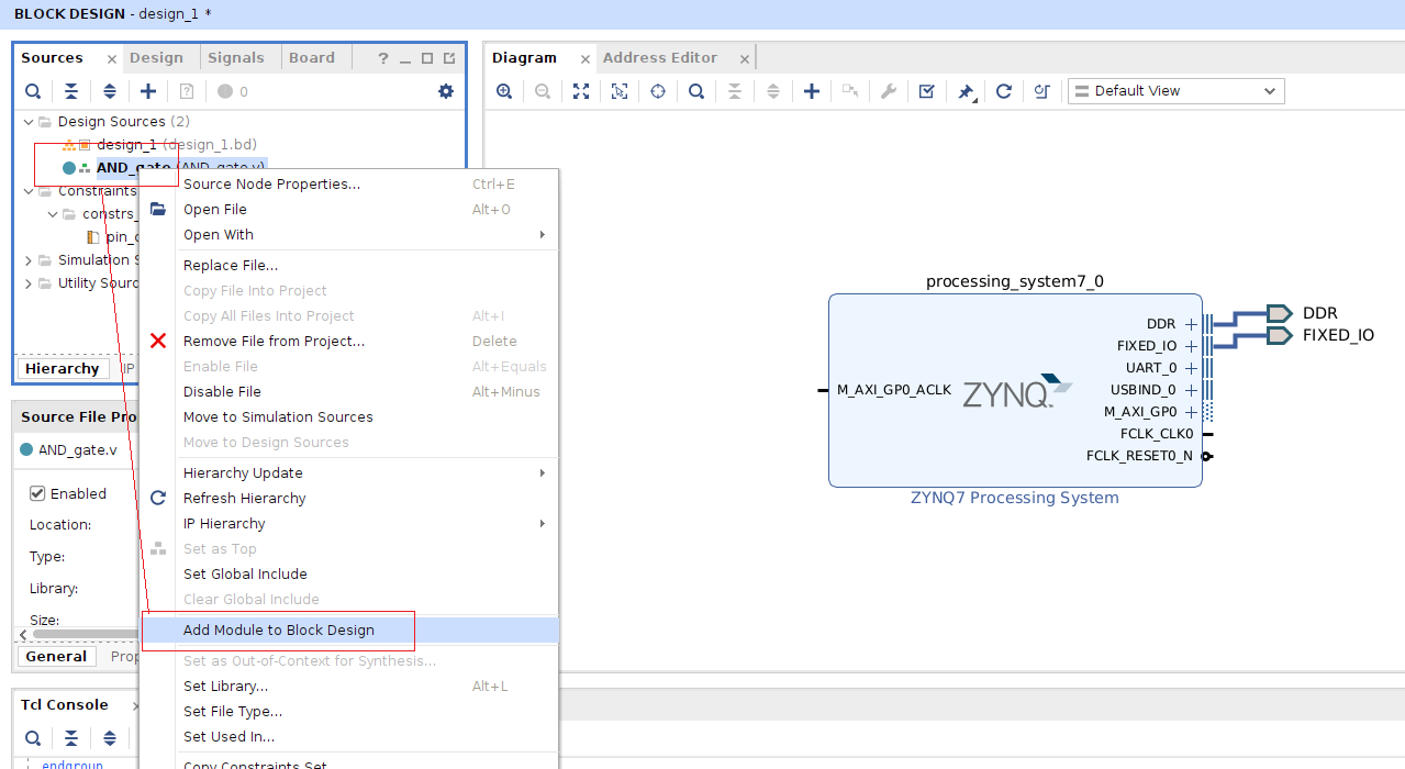
In this stage I will add the AND gate to this block design. We wrote the verilog code for the AND gate. To add it as a block we need to select Add Module to Block Design.
The AND gate Block is added.
For controlling the GPIO using the Processing system we need to add the AXI GPIO interface.
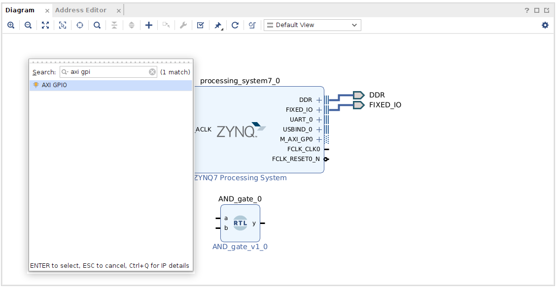
I added two AXI GPIO block in my design.
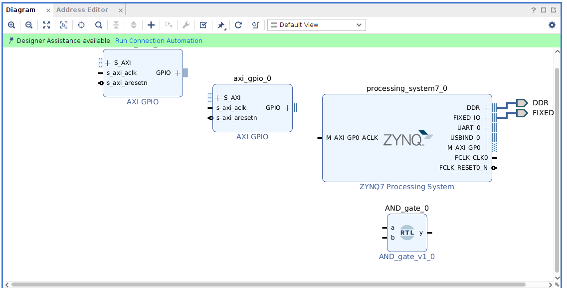
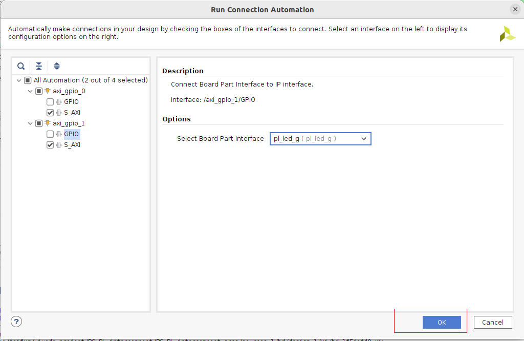
The we need to run the connection automation again. Select all without GPIO because we make those connection manually.
This is the connections after adding axi_gpio interface. AND gate is not added to the system yet.
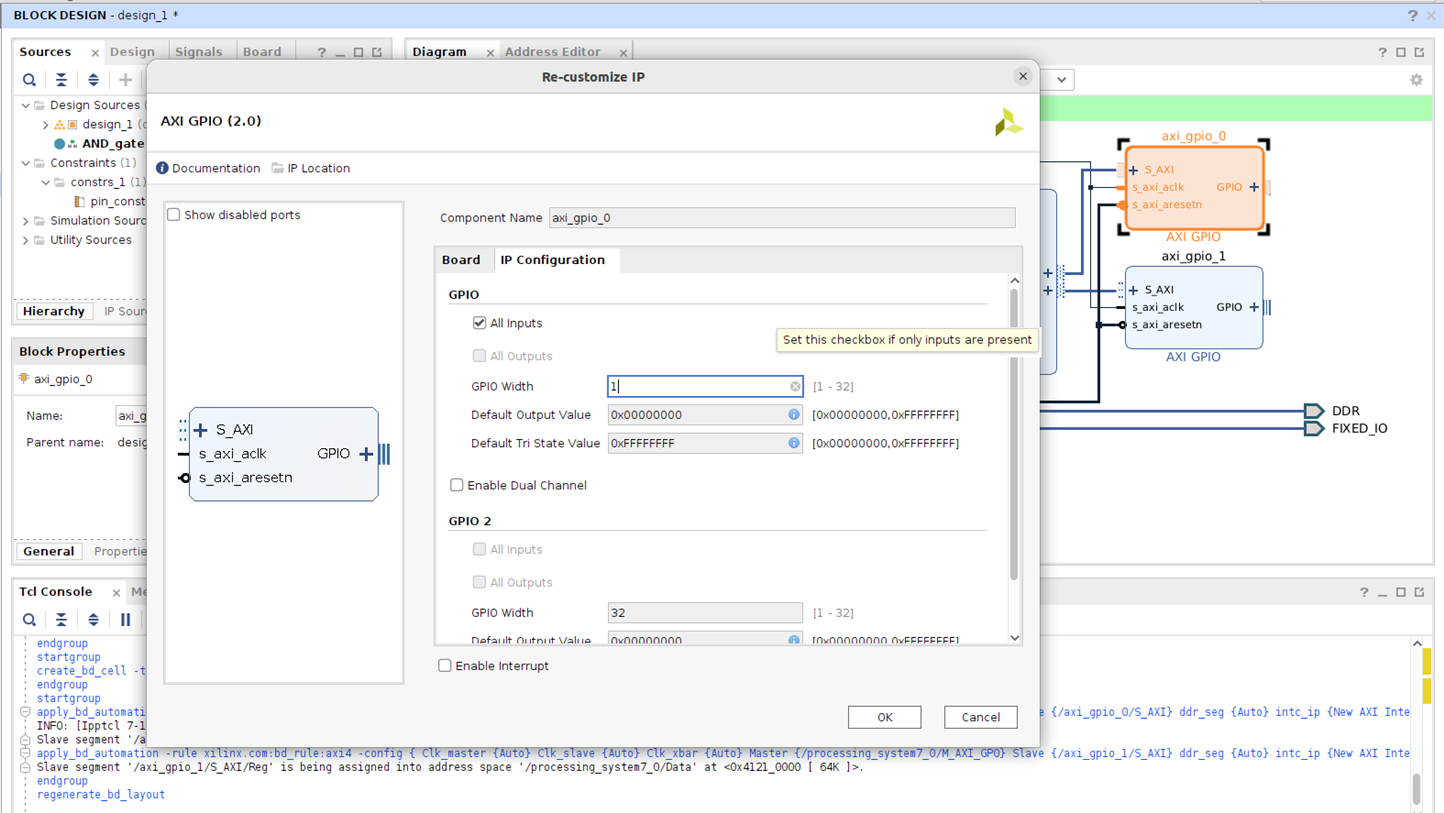
But before that we need to configure the axi_gpio block as follows. This is the configuration for axi_gpio_0.
Then the following connection is made with the output of the AND module.
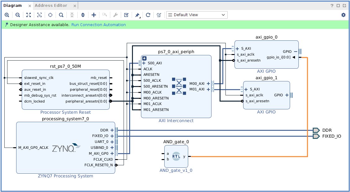
Input a and b of the AND block is marked as external and renamed as sw0 and sw1.
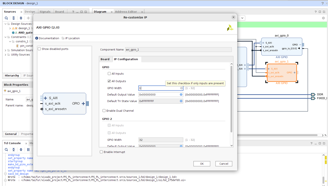
Axi_gpio_1 is configured as follows.
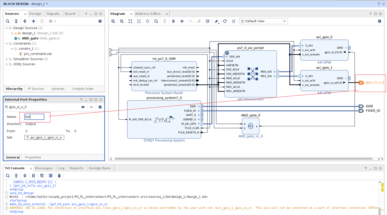
The external pin is marked as led.
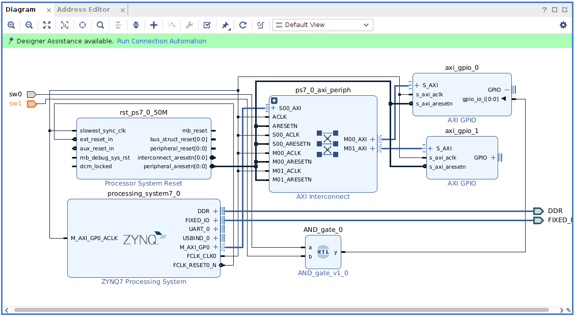
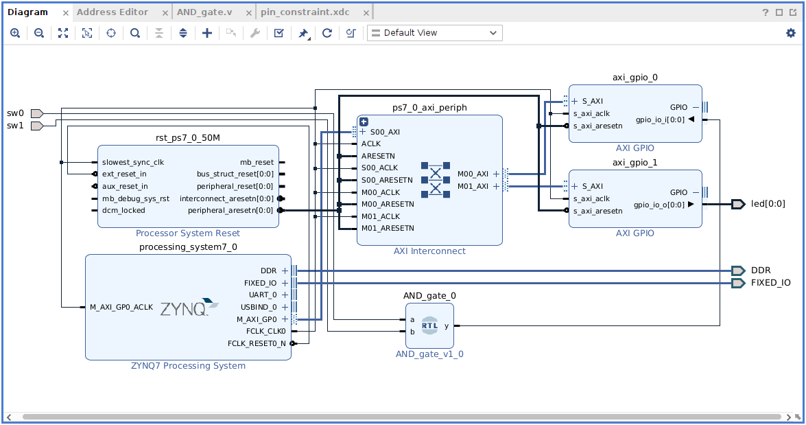
This is the final block design.
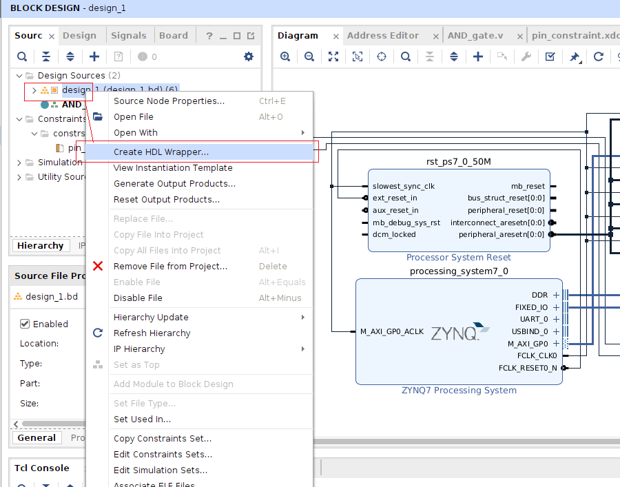
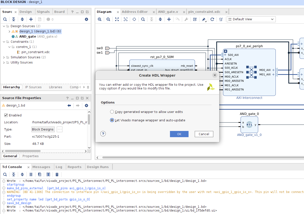
Now we need to create the HDL Wrapper of the block design. Right click on the desing and click on Create HDL Wrapper.
Choose the following option and click OK.
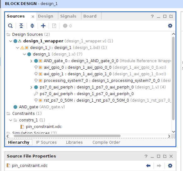
After successful creation of the HDL Wrapper you will see the following design resources.
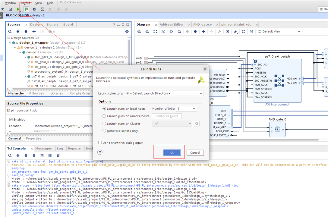
The next step is to generate the Bitstream. Click the menu button and click OK.
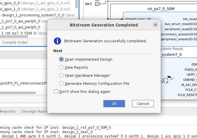
You will get following confirmation after generation of the bitstream.
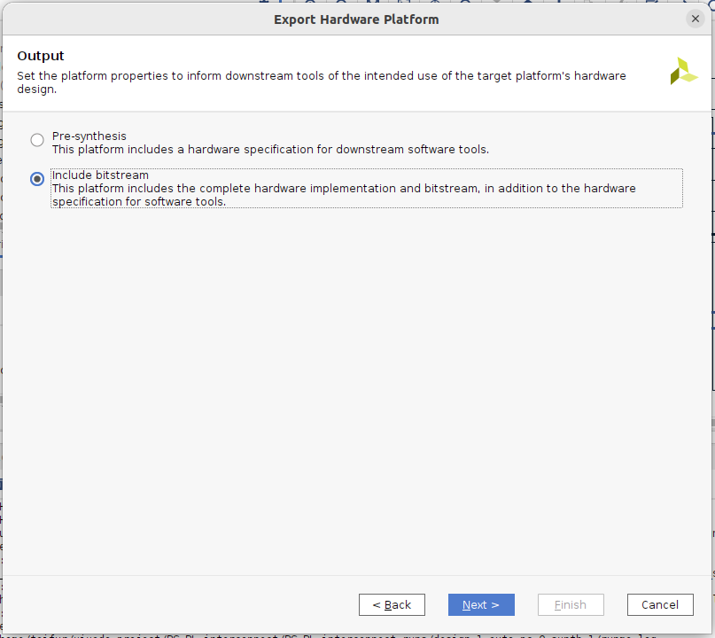
Now we will export our hardware design.
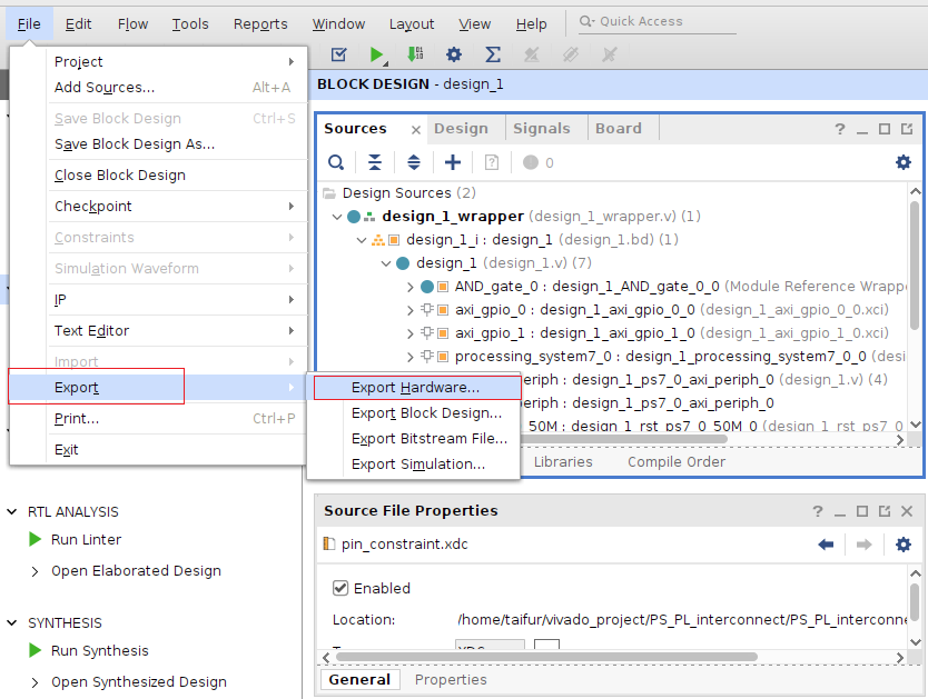
Include bitstream and click Next.
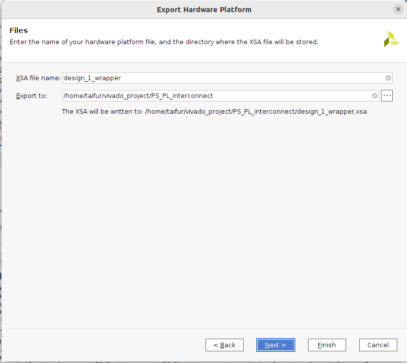
Chose the name and directory for XSA file.
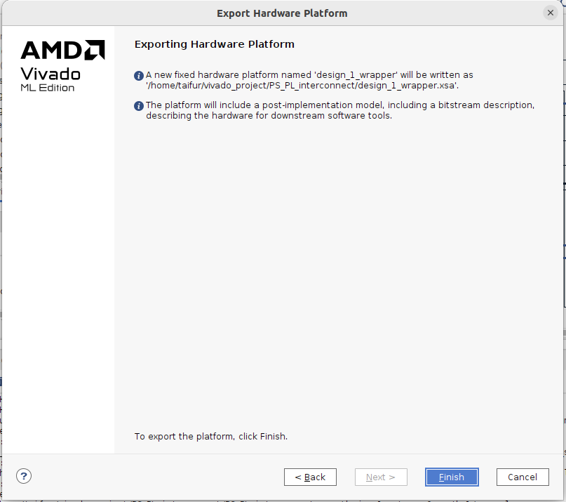
Finally click on Finish.
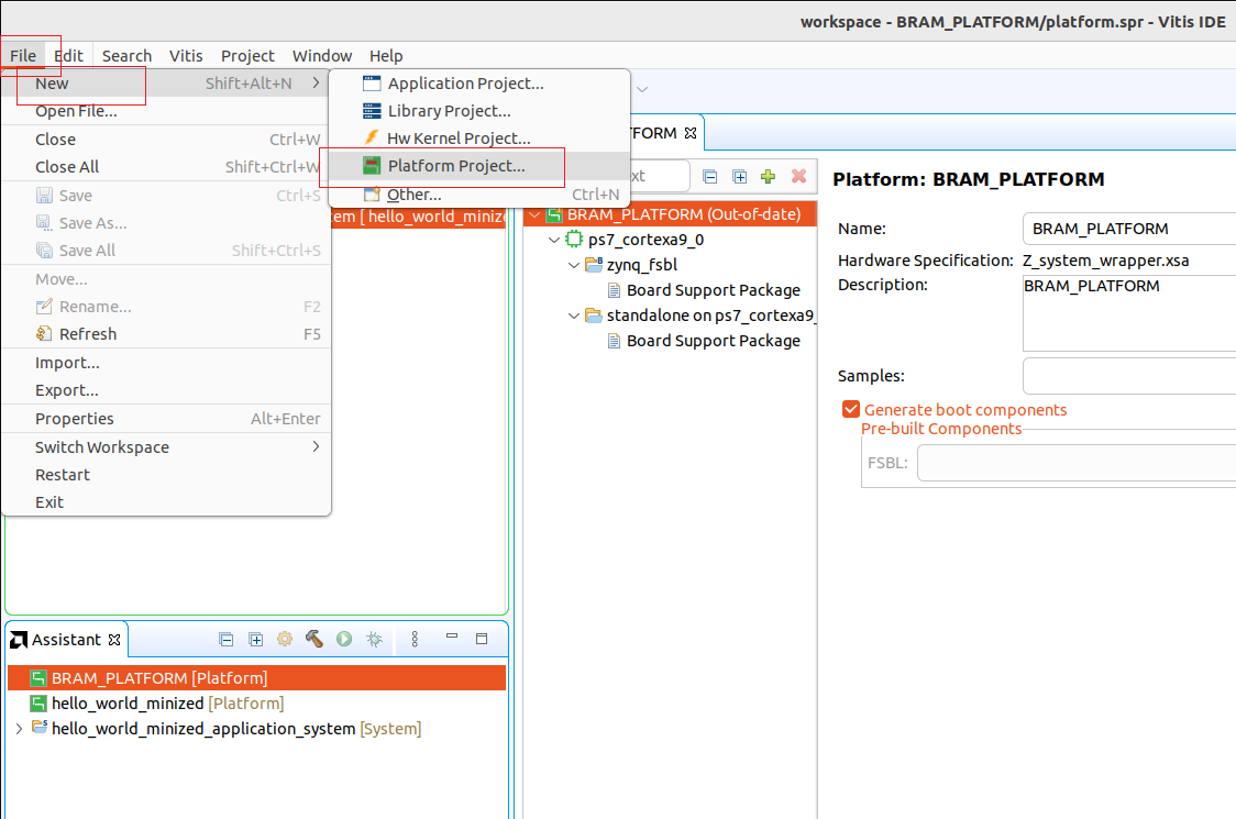
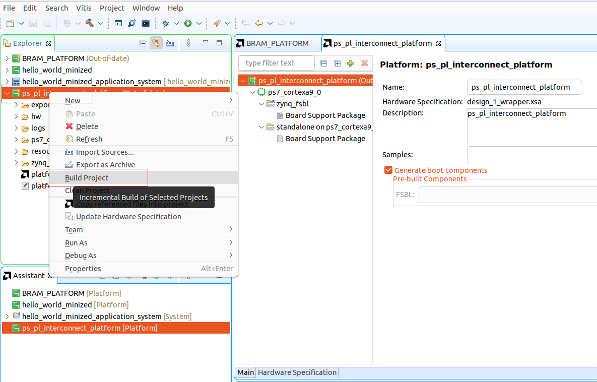
Our hardware design is successfully created. We will now create application for the processing system. We need to open Vitis for creating the application. After running the Vitis first we need to open our hardware desing as platform project.
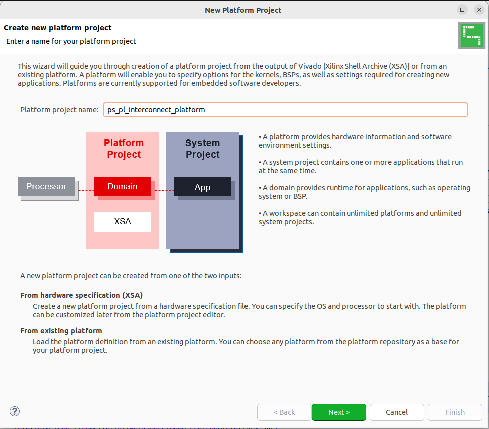
We need to choose a name for the platform project and click the Next.
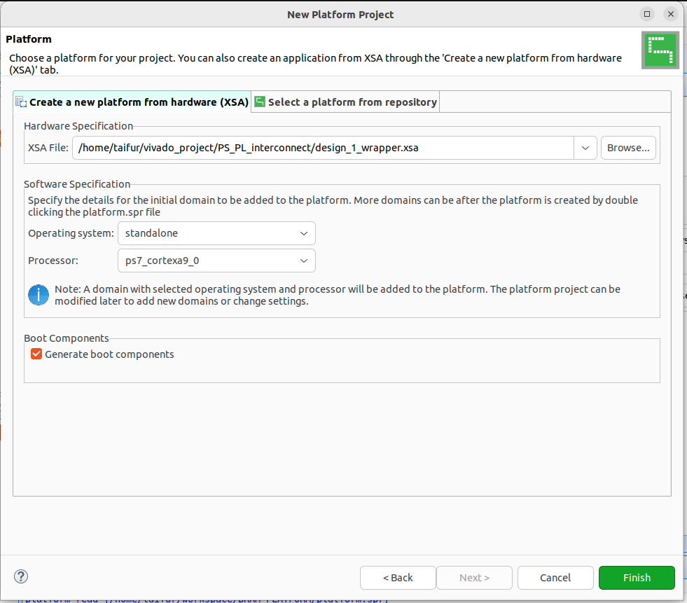
Then we need to locate the hardware XSA we save before from the Vivado and click Finish.
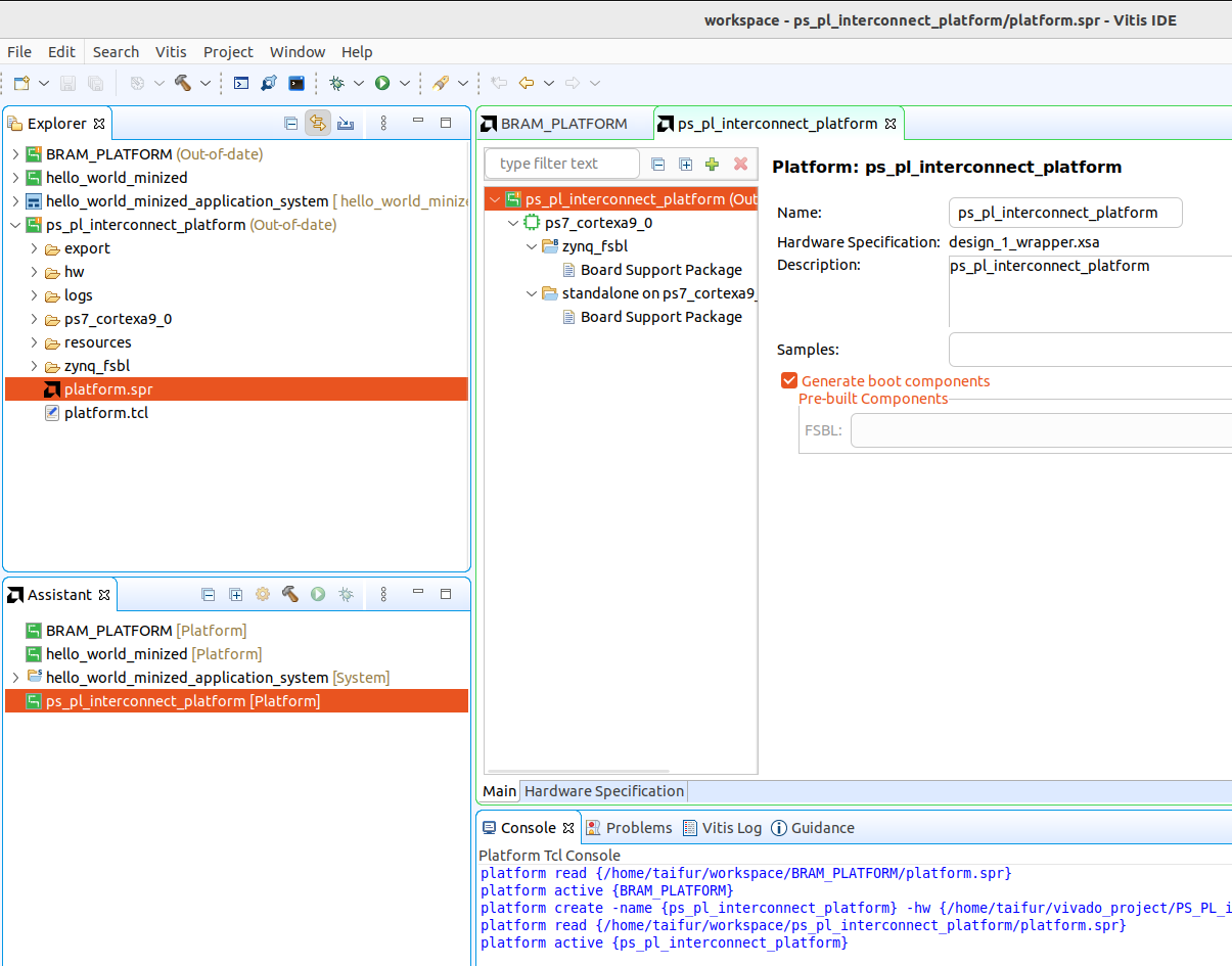
The hardware design is successfully imported.
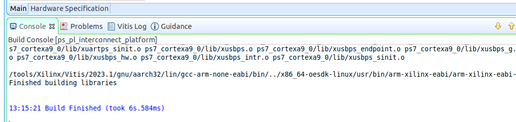
Now we will build the hardware design.
The design is build successfully.
Now we will create an application project for the zynq processing system.
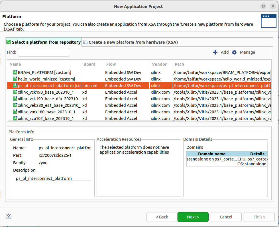
Select the right platform in this stege.
Create a name for the application.
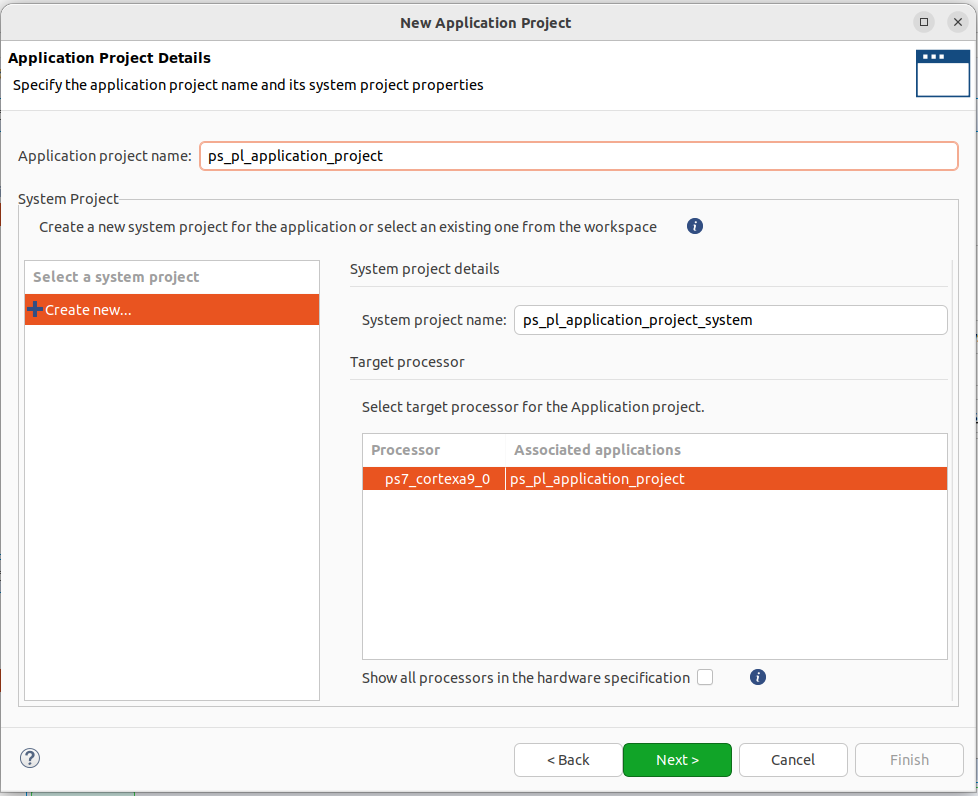
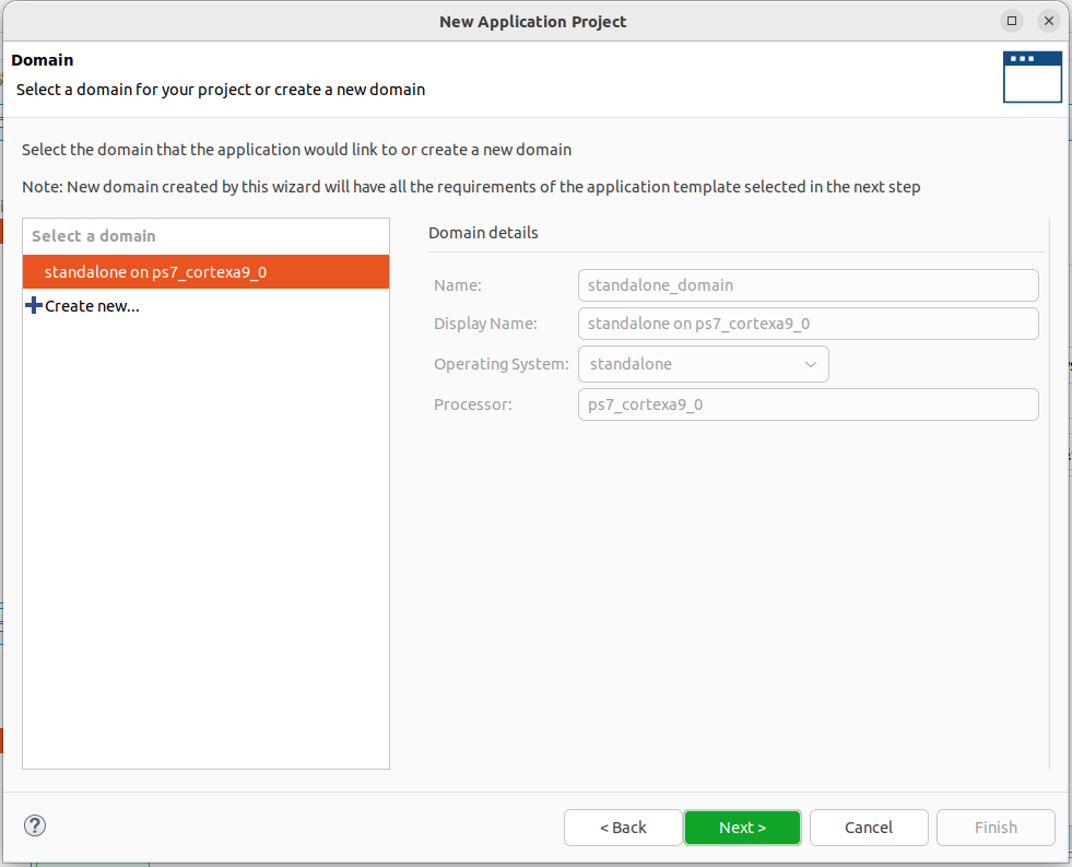
Click on Next.
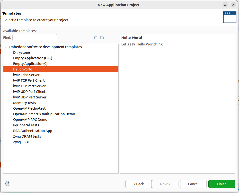
Create Hello World template:
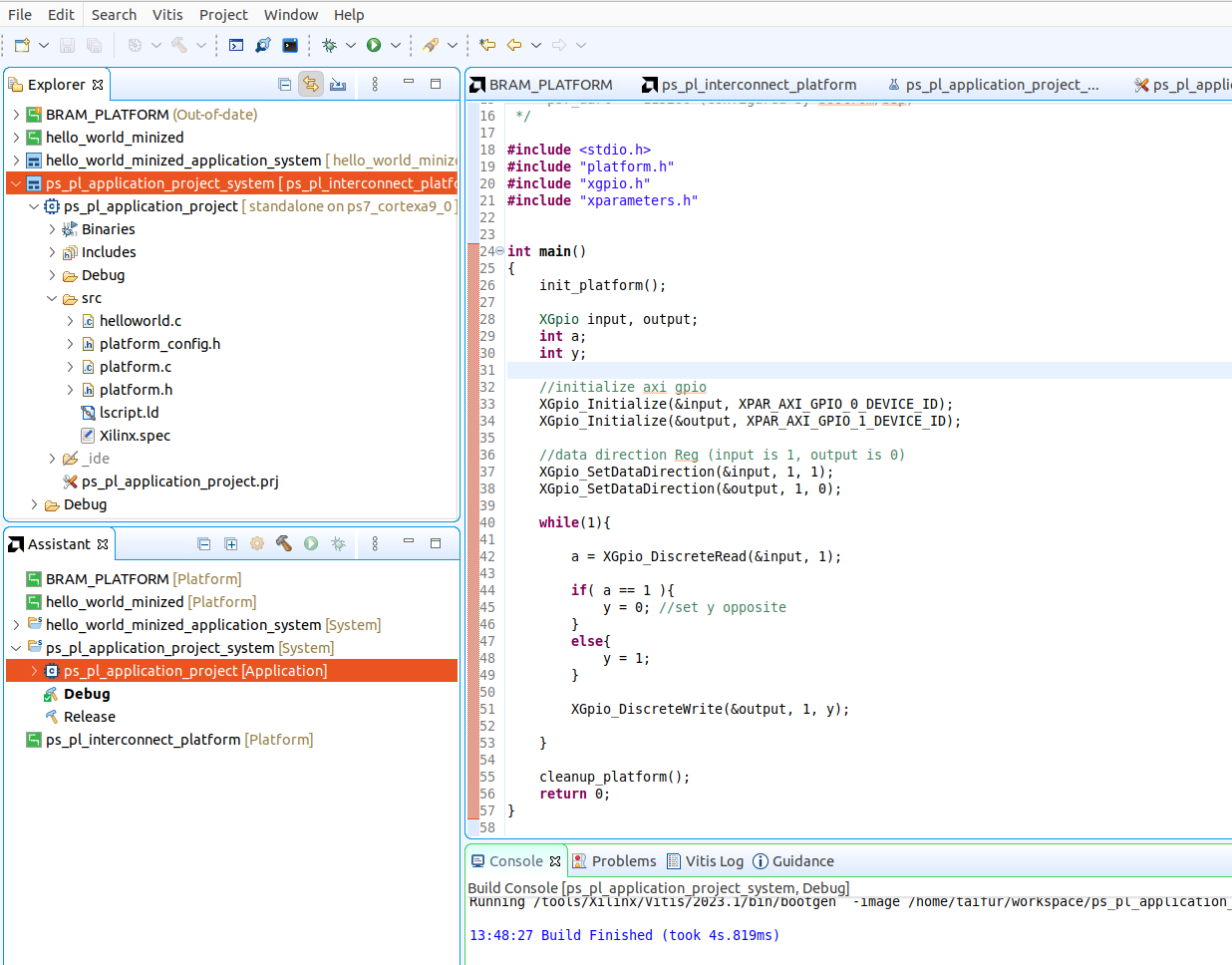
Open the helloworld.c source file and add your code. Add the following code in the source file.
/*
 * helloworld.c: simple test application
 *
 * This application configures UART 16550 to baud rate 9600.
 * PS7 UART (Zynq) is not initialized by this application, since
 * bootrom/bsp configures it to baud rate 115200
 *
 * ------------------------------------------------
 * | UART TYPE   BAUD RATE                        |
 * ------------------------------------------------
 *   uartns550   9600
 *   uartlite    Configurable only in HW design
 *   ps7_uart    115200 (configured by bootrom/bsp)
 */

#include <stdio.h>
#include "platform.h"
#include "xgpio.h"
#include "xparameters.h"


int main()
{
    init_platform();

    XGpio input, output;
    int a;
    int y;

    //initialize axi gpio
    XGpio_Initialize(&input, XPAR_AXI_GPIO_0_DEVICE_ID);
    XGpio_Initialize(&output, XPAR_AXI_GPIO_1_DEVICE_ID);

    //data direction Reg (input is 1, output is 0)
    XGpio_SetDataDirection(&input, 1, 1);
    XGpio_SetDataDirection(&output, 1, 0);

    while(1){

    	a = XGpio_DiscreteRead(&input, 1);

    	if( a == 1 ){
    		y = 0; //set y opposite
    	}
    	else{
    		y = 1;
    	}

    	XGpio_DiscreteWrite(&output, 1, y);

    }

    cleanup_platform();
    return 0;
}
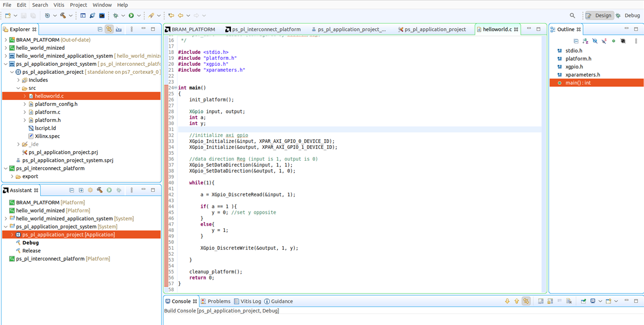
And finally build your code.
Top Comments
-

rohini
-
Cancel
-
Vote Up
0
Vote Down
-
-
Sign in to reply
-
More
-
Cancel
-

javagoza
in reply to rohini
-
Cancel
-
Vote Up
+1
Vote Down
-
-
Sign in to reply
-
More
-
Cancel
Comment-

javagoza
in reply to rohini
-
Cancel
-
Vote Up
+1
Vote Down
-
-
Sign in to reply
-
More
-
Cancel
Children