


Hello Everyone, My peers in Path to Programable have Done Great work in giving step by step procedure to implement DMA transfer so Why Reinvent the Wheel , I take a different approach.
I will try to present a vivid picture regarding Why we need to implement few IPs to achieve DMA transfer between BRAM and DDR instead of using PS and How?
First As always we take Bottom Up approach , Fasten your Seat Belts !
What is DMA ?
DMA refers to Direct Memory Access , which in short is used to releive the PS from the Burden of Transfering Data from Memory (DDR in this case)
to other I/O device (BRAM in PL for this case) , so that PS may do other important tasks , It also reduces the possible length of the Path through which Data will travese.
So DMA is simply a peripheral device/Functional Block which requires the Source Address and Destination Address with the Size of Block of Data to transfer.
What is Block RAM (BRAM)?
It is some Dedicated Portion in PL section where only memory structures are fabricated which is different from logical block(slice) in PL where other elements (Mulltiplexers/LUTs , FlipFlops ) are present.It is made so that we don't waste a Logical Block for storing Data.
Functionally a BRAM is used for storing Blocks of Data , It can also be used as a FIFO between PL and PS blocks and other only when we use it with help of a Controller which is responsible for synchronizing reading and writing data in BRAM.
So a BRAM is just some bunch or Raw space for Bits and the BRAM controller is the Brain which uses the Space for our Needs .
Implementation:
In minized we implement it on PL fabric by using BLOCK MEMORY GENERATOR IP which creates the space (for bunch of data in blocks) and also the Controller where we selected Dual Port so that we can Read Data from One End and Write Data into it from Other End (more flexible than a FIFO) and also use it as a DDR for PL blocks to Process Data.
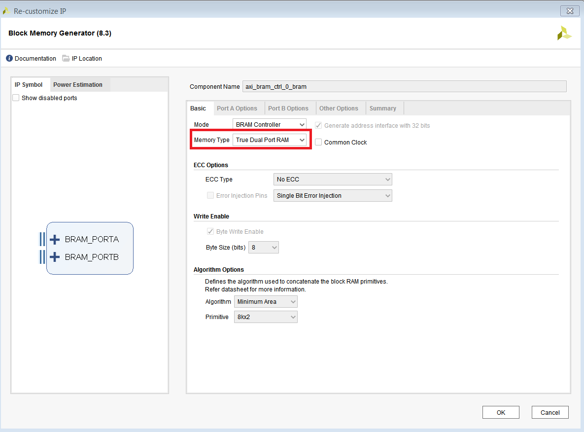
1.)In your Existing project just go for add IP and type "GENERATOR" and select the "BLOCK MEMORY GENERATOR IP"
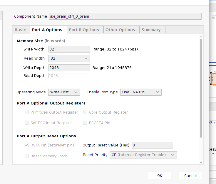
Configure the Controller as you wish based on your Requirement , For instance I used these settings :
2.)
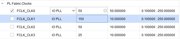
a.)Reconfigure "ZYNQ7 PROCESSING SYSTEM" ip block to Enable Fabric Clock 'FCLK_CLK0' in 'Clock Configuration' section for PL (every system needs clock Isn't It) and
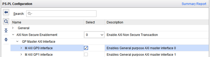
b.)Enable 'M AXI GP0 Interface' in 'PS-PL Configuration'
3.)Add Another IP "AXI BRAM CONTROLLER" and configure it based on above settings (for Instance)as shown below :
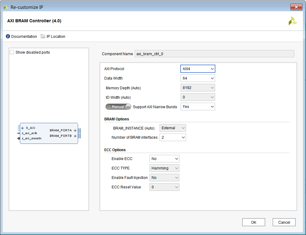
What Is this AXI ?
AXI is simply a bus Standard in which there will be a master and slave , the master generates the control signals to decide when to transfer or allow slave to send Data , we use multiple masters and slaves by means of AXI interconnect(we will see it).
What is This AXI BRAM CONTROLLER used for ?
It acts as a Bridge to connect PS to BRAM Controller, since we are using AXI bridge we need to make sure BRAM Controller to understands AXI's language , so we add this IP to our Design.
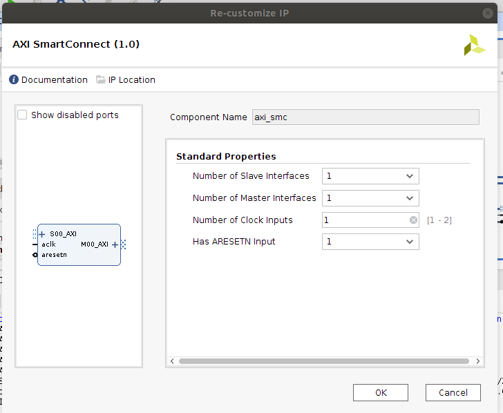
4.) Add 'AXI Interconnect' (If you got More Devices) or 'AXI smart connect' (for single device) IP in your Design to connect the Master AXI of PS connect to the above PL blocks seen as Slaves .In my case i sort for AXI Smart Connect (because Small Work Isn't It  ):
):
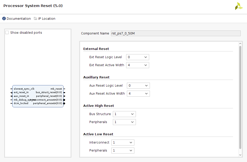
5.)Add "Processor System Reset" IP which is neccesary to prevent crazy things to happen and Synchronize it by reseting PL blocks to some known state
How they Work ?
For Eg. Consider you want to Add data read by MEMS sensor connected to PS whose Data stored in DDR using Adders implemented in PL.
On starting the minized the "Processor System Reset" resets the PL,AXI(other peripherals if any) and maintain them in a predefined state until PS starts up and running.
Since data is continuously generated from Sensor we can use BRAM Controller in PL to store data to process by Adder in PL logic .
We connect the DDR through PS to 'BRAM Controller' through AXI Interconnect(or smart connect) and 'AXI BRAM Conroller' and transfer that Data to BRAM Port A and this Data is used by Adder Logic in PL through Port B of BRAM ,In this way a Dual Port BRAM can be used in Variety of ways and it makes our lives easier
Exporting the Hardware
Validate the design ->Reset Output Products and then Generate Output Product under the sources and the SystemWrapper
Generate Bitstream -> Export Hardware to SDK workspace
Launch SDK with the same location mentioned as workspace (where we stored Bitstream)
SDK Part Folks !
1.)In SDK, Create a New BSP -> Import your previous peripheral projects for using those devices such as UART for serial communication
2.)Create a new application project (File ->New -> Application Project)
3.)Enter BRAM_DMA_Test for the Project name and select Use existing for the BSP. Click NEXT ->Select Empty Application ->Finish.
4.)Then Import the BRAM program code(attached below) into your Project src by:
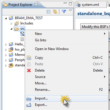
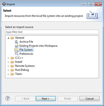
Select the Path where you stored the "dma_test.c" attached here and select this file -> Finish
Running The Program
1.)Connect Minized to computer
2.)Program the FPGA ( PL ) :
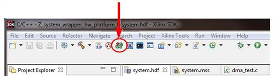
Then Go for Default options -> Program
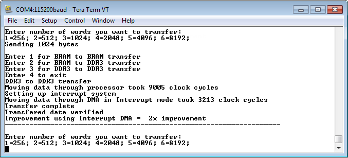
3.)Open Serial Terminal like Putty or Teraterm at 115200 baud rate
4.)Right-click on BRAM_DMA_Test and select Run As ->Launch on Hardware (System Debugger)
5.)Once the code is downloaded to the board, TeraTerm/Putty should show the burst size prompt.
That's It
Meet you guys in my Next Post , where we will create a Custom IP for Ourselves.
Feel Free to Comment !
Top Comments
-

DAB
-
Cancel
-
Vote Up
+2
Vote Down
-
-
Sign in to reply
-
More
-
Cancel
Comment-

DAB
-
Cancel
-
Vote Up
+2
Vote Down
-
-
Sign in to reply
-
More
-
Cancel
Children