


Note: This is part 2 of a series on working with FPGAs and in particular the Xilinx Zynq-7000S Programmable System-on-Chip with ARM Cortex-A9 processing core. For part 1, click here: Xilinx ZYNQ System-on-Chip - Getting to know the MiniZed Board
For all parts, click here: Path to Programmable
- Introduction
- Creating an Example Project
- Zynq-7000 Programmable Logic and DSP Scale
- Exploring Vivado
- Adding the Processor System
- Configuring the Processing System
- A Glimpse of VHDL: Wrapper for the Processing System
- Building the Design
- Exploring the Design
- Software Development Environment (Xilinx SDK)
- Creating a Software Project
- Running the Project
- Summary
Introduction
This blog post is part of the Path to Programmable series. It documents my journey as a beginner with a Xilinx Programmable System-on-Chip which contains programmable logic and an ARM Cortex-A9 processor system. It comes on a development board called MiniZed.
In the previous blog post the MiniZed board was introduced. This blog post covers my experience with the first couple of training sessions. I’m rarely really impressed at the pace of training courses, but I have to say I was really impressed this time. It was like taking the red pill in the Matrix : ) It was like discovering a wormhole. I got further in a few hours than I imagined possible!
If you’re interested in using programmable SoCs, it is highly recommended to pick up a MiniZedMiniZed and try to join in, so we can bounce ideas off each other during the next two months.
I have to be careful not to trivialize the effort, because a lot was covered in a couple of the virtual training sessions. And I’m aware there is a huge journey to continue on. However, I was happy with the initial progress made so far – it was a big leap, and worth it.
So, this blog post covers the big leap (for me at least), hopefully in a concise and understandable way if anyone wants to follow along. Hopefully combined with the rest of the virtual Path to Programmable team’s blog posts, things should make sense.
What is the big leap? It is getting from a fresh Programmable SoC chip to the situation that it is successfully interfaces to DDR3 RAM and some C code is running inside the SoC’s processor and generating console output over a UART. This blog post discusses how all that was achieved from scratch, using Xilinx Vivado 2017.4 HLx WebPack and the MiniZed board. If you wish to follow along and replicate, then the software can be downloaded for free from the Xilinx website.
Creating an Example Project
Once Vivado was installed, I fired it up and created a project selecting VHDL as the language that would be used. You can use the screenshots below to do this if you’re following along (click to zoom the screenshot).

The precise Zynq part also needs to be specified when using the Create Project wizard. To find that out, the MiniZed hardware documentation can be consulted and it specifies the part as XC7Z007S-1CLG225C.

According to the Zynq-7000 PDF datasheet, that indicates a speed grade 1 part, in CL package, with 225 pins and commercial temperature range. This information was used to select the correct part in the Create Project wizard, although it specifies the part code as xc7z007sclg225-1 once the correct family, package and speed has been selected.
Zynq-7000 Programmable Logic and DSP Scale
There are 10 devices in the Zynq-7000 range, each with various speed grades and operational temperature ranges. They are lined up in the chart below to get a rough idea about the scale across the range. From left to right, the first three are have a single-core processor and the remainder are dual-cored. In terms of programmable logic (PL) and blocks of memory available to the PL, there is more than tenfold increase across the range. The MiniZed board uses the leftmost, smallest device in the range.

There is more than 30 times the DSP performance (see the DSP Slices and DSP GMAC bars in the chart above) going from left to right.
I doubt I’m going to be pushing the limits of the MiniZed : ) but it is nice to know that there are members of the Zynq-7000 for massively larger designs too. It is one of the great benefits of programmable logic, that it can be scaled in huge ways (allowing for parallel processing of data).
Exploring Vivado
Once the project was created, the panes for Vivado appeared as shown below. The key areas that were later used are highlighted. The left area, under Project Manager, contains various tasks that need, mainly from top to bottom, but tasks can be skipped and the system will automatically run any previous tasks that are dependant on the current task.
The bottom area mainly contains reports and log output. From what I can see, it looks like Vivado’s tasks have an API in TCL, and therefore the Design Suite may not be essential; it could be possible to script everything in TCL for power users. I’m just speculating until I know more!
The main body of the Design Suite, circled in green, initially shows the Project Summary after the Create Project wizard was executed, but it can show many other things as will be discovered later. The red circled area shows a symbol which means ‘expand all’. It is sometimes clicked, within other windows that may appear when the Design Suite is used.
In summary I was pleasantly surprised that on initial appearance, Vivado didn’t seem as scary as the quite abstract name suggests! It all seemed logical.

Adding the Processor System
The next step was to add the processor to the design. Vivado treats it like any other design component (known as intellectual property or IP). Vivado comes equipped with perhaps 200 different IP components, including things like digital audio blocks, video blocks and of course the processor subsystem. IP in general is a great resource because it should be guaranteed working programmable hardware components!
IP in the FPGA world is like the digital logic equivalent of vendor code libraries in the computer software world. Adding (say) a video block IP into the design will allow a complete hardware state machine and other digital logic that would implement the video function to be available in the FPGA. For this initial exercise, just the processor subsystem IP is added.

Once the Create Block Design task is clicked and a name is given to the design block being created, the ‘+’ icon can be clicked in the main large pane, and a large list of available IP is shown. It can be searched and the Processing System found and double-clicked.
It was very cool that a graphical object then got placed in the center pane. The green bar above it allows the object (the Processing System) to be configured!
It can be imagined that the configuration needed will include things like configuring what type of memory is attached to the Zync SoC, and also adding any peripherals that could be desired, such as serial buses to complete the processor system. All that is done by clicking on the Run Block Automation text in the green bar.
Configuring the Processing System
As discussed, the configuration of the processing system entails doing things like configuring the memory, clock and I/O, to get a fully functioning compute capability for the Zync SoC. By clicking through, it was very quick to get to a nice graphical diagram which showed all the possible things that could be configured.

Any of the pink items in the block diagram could be clicked on to configure them, or the list just to the left of the diagram could be used. The blue circled item gets you back to the block diagram. At a minimum, things like the clock and memory need configuring. The pink circled items were configured, and they are discussed below.
Configuring the UART
A single asynchronous serial interface (known as a UART) was configured. This is the near-standard way to access any computer in the absence of a graphical user interface. Often electrically they are based on the RS232 standard on a full computer, but in the case of small processor chips, the voltage levels are quite often set to 3.3V. The UART can be brought out to different possible pins, so the configuration system allows the pins to be chosen (much like other ARM chips, there are only finite combinations available, so it is highly recommended to configure things from the left-side list in top-down order, to get the most awkward items configure first). After it was all completed, a tiny check-mark was visible on the green block diagram, showing that UART1 in this case was configured.

Another part of the UART is configured in the General Settings area of the block diagram, which is part of the PS-PL (Processing System to Programmable Logic) configuration. There, the baud rate was confirmed to be 115200.
This was all surprisingly smooth, and I can’t imagine how it could be simplified further by Xilinx.
Configuring the Clocks
Moving on down the list of stuff to be configured to enable the processing system to function, the next thing was to configure the clocks. Most processors internally have several clocks (all generated from a single external clock) implemented using a technology known as phased locked loops (PLL). This allows for the external clock to be multiplied or divided inside the chip, to clock different parts of the chip at different rates. This allows for slow things (like long connections off-chip to perform input/output) to run at a slower (and hence more energy-efficient) speed compared to the things that can be run at far higher rates (such as memories close to the chip). Some things like DDR memory require clocks within certain ranges, otherwise data is corrupted.

For the current exercise, since the programmable logic (PL) portion is unused, the clock to it is disabled and the interface is disconnected. The last couple of steps in the screenshots above are used to perform the disabling.
Configuring the Memory (RAM)
The final bit of mandatory config to get the processor system functioning is to set up the memory access details. In the case of the MiniZed board, this consists of instructing Vivado that DDR3 memory is on-board, and specifying the part details (custom information can also be configured if the memory chip was an unusual one). Delay settings are configured so Vivado is aware of PCB trace lengths out to the high speed memory.

Once it is all configured and saved, in the main pane the graphical design can be validated. Once that’s done, we’re actually ready to work with the very first piece of VHDL!
A Glimpse of VHDL: Wrapper for the Processing System
Now that the IP for the Processing System has been fully configured, it is time to let Vivado create some VHDL code for it. This was quite straightforward, it is just a few clicks! At the end of the process, the generated file (in this case Z_system_wrapper.vhd because at the start of this exercise we gave the IP the name Z_system) can be double-clicked and the main pane will display the VHDL output with syntax highlighting.

Just for reference, the entire VHDL output is listed here – it is described further below.
--Copyright 1986-2017 Xilinx, Inc. All Rights Reserved.
----------------------------------------------------------------------------------
--Tool Version: Vivado v.2017.4 (win64) Build 2086221 Fri Dec 15 20:55:39 MST 2017
--Date        : Mon Oct 22 01:38:58 2018
--Host        : DESKTOP-SHABAZ1 running 64-bit major release  (build 9200)
--Command     : generate_target Z_system_wrapper.bd
--Design      : Z_system_wrapper
--Purpose     : IP block netlist
----------------------------------------------------------------------------------
library IEEE;
use IEEE.STD_LOGIC_1164.ALL;
library UNISIM;
use UNISIM.VCOMPONENTS.ALL;
entity Z_system_wrapper is
  port (
    DDR_addr : inout STD_LOGIC_VECTOR ( 14 downto 0 );
    DDR_ba : inout STD_LOGIC_VECTOR ( 2 downto 0 );
    DDR_cas_n : inout STD_LOGIC;
    DDR_ck_n : inout STD_LOGIC;
    DDR_ck_p : inout STD_LOGIC;
    DDR_cke : inout STD_LOGIC;
    DDR_cs_n : inout STD_LOGIC;
    DDR_dm : inout STD_LOGIC_VECTOR ( 1 downto 0 );
    DDR_dq : inout STD_LOGIC_VECTOR ( 15 downto 0 );
    DDR_dqs_n : inout STD_LOGIC_VECTOR ( 1 downto 0 );
    DDR_dqs_p : inout STD_LOGIC_VECTOR ( 1 downto 0 );
    DDR_odt : inout STD_LOGIC;
    DDR_ras_n : inout STD_LOGIC;
    DDR_reset_n : inout STD_LOGIC;
    DDR_we_n : inout STD_LOGIC;
    FIXED_IO_ddr_vrn : inout STD_LOGIC;
    FIXED_IO_ddr_vrp : inout STD_LOGIC;
    FIXED_IO_mio : inout STD_LOGIC_VECTOR ( 31 downto 0 );
    FIXED_IO_ps_clk : inout STD_LOGIC;
    FIXED_IO_ps_porb : inout STD_LOGIC;
    FIXED_IO_ps_srstb : inout STD_LOGIC
  );
end Z_system_wrapper;


architecture STRUCTURE of Z_system_wrapper is
  component Z_system is
  port (
    DDR_cas_n : inout STD_LOGIC;
    DDR_cke : inout STD_LOGIC;
    DDR_ck_n : inout STD_LOGIC;
    DDR_ck_p : inout STD_LOGIC;
    DDR_cs_n : inout STD_LOGIC;
    DDR_reset_n : inout STD_LOGIC;
    DDR_odt : inout STD_LOGIC;
    DDR_ras_n : inout STD_LOGIC;
    DDR_we_n : inout STD_LOGIC;
    DDR_ba : inout STD_LOGIC_VECTOR ( 2 downto 0 );
    DDR_addr : inout STD_LOGIC_VECTOR ( 14 downto 0 );
    DDR_dm : inout STD_LOGIC_VECTOR ( 1 downto 0 );
    DDR_dq : inout STD_LOGIC_VECTOR ( 15 downto 0 );
    DDR_dqs_n : inout STD_LOGIC_VECTOR ( 1 downto 0 );
    DDR_dqs_p : inout STD_LOGIC_VECTOR ( 1 downto 0 );
    FIXED_IO_mio : inout STD_LOGIC_VECTOR ( 31 downto 0 );
    FIXED_IO_ddr_vrn : inout STD_LOGIC;
    FIXED_IO_ddr_vrp : inout STD_LOGIC;
    FIXED_IO_ps_srstb : inout STD_LOGIC;
    FIXED_IO_ps_clk : inout STD_LOGIC;
    FIXED_IO_ps_porb : inout STD_LOGIC
  );
  end component Z_system;
begin
Z_system_i: component Z_system
     port map (
      DDR_addr(14 downto 0) => DDR_addr(14 downto 0),
      DDR_ba(2 downto 0) => DDR_ba(2 downto 0),
      DDR_cas_n => DDR_cas_n,
      DDR_ck_n => DDR_ck_n,
      DDR_ck_p => DDR_ck_p,
      DDR_cke => DDR_cke,
      DDR_cs_n => DDR_cs_n,
      DDR_dm(1 downto 0) => DDR_dm(1 downto 0),
      DDR_dq(15 downto 0) => DDR_dq(15 downto 0),
      DDR_dqs_n(1 downto 0) => DDR_dqs_n(1 downto 0),
      DDR_dqs_p(1 downto 0) => DDR_dqs_p(1 downto 0),
      DDR_odt => DDR_odt,
      DDR_ras_n => DDR_ras_n,
      DDR_reset_n => DDR_reset_n,
      DDR_we_n => DDR_we_n,
      FIXED_IO_ddr_vrn => FIXED_IO_ddr_vrn,
      FIXED_IO_ddr_vrp => FIXED_IO_ddr_vrp,
      FIXED_IO_mio(31 downto 0) => FIXED_IO_mio(31 downto 0),
      FIXED_IO_ps_clk => FIXED_IO_ps_clk,
      FIXED_IO_ps_porb => FIXED_IO_ps_porb,
      FIXED_IO_ps_srstb => FIXED_IO_ps_srstb
    );
end STRUCTURE;
It is not a lot of code; just 91 lines, which define a VHDL Design Entity or Module. In this case, the entity or module happens to be the processor system. The diagram here shows a graphic representation of a typical VHDL design entity.

It consists of an entity declaration portion (the red part of the diagram), which defines only the external input/output connections from the module.
The rest of the file contains the architecture body, that is responsible for explaining the internals of the design entity. To do that, there are several methods possible in VHDL. One method is to declare what components are used and the names of the component pins. It is shown in blue. The connections between components, and to the outside world, are defined in the final portion shown in orange.
The two part architecture that uses component declarations and component instantiations, is known as a structural model. As mentioned there are other ways of defining the architecture. Vivado describes the processor system using a structural model.
With that information, the 91 lines of content begin to make sense. It can be seen that the file contains one component that is instantiated to create the VHDL design entity. The connections are things like the DDR memory bus, input/output pins, a reset line and a processor clock.

Building the Design
This part of the process converts everything into a hardware implementation ready for execution. In Vivado, everything in the left pane (the Flow Navigator) occurs sequentially. So by clicking on Generate Bitstream which is toward the bottom of the Flow Navigator pane, Vivado will execute everything else needed to achieve that. It would have been nice to see the software show an animation near each step (like the older Xilinx ISE software) but instead it is possible to see how far things have progressed by looking out for some text that changes at the top-right of the Vivado Design Suite.

Once the bitstream has been created (it will be a file called Z_system_wrapper.bit in this case), now the time has almost come for the hardware designer to hand off to the software developer to do their bit.
The software developer will want to be able to write, compile and run software in a programming language such as C. To do that, the developer needs more than the bitstream. Enough information is needed for the software development environment to be able to create startup code that will initialize the ARM processor and get things ready for executing the main code. To allow all this to occur, the hardware engineer needs to do one more thing and that is to click on File->Export->Export Hardware. This will generate some files that the software development environment can use to auto-generate the startup code which will initialize the processor in software to work with the memory and so on. Also, the bitstream can be included in the bundle of files so that the software developer can test the code for real on the hardware.
Exploring the Design
Before looking at the software developer’s tasks, I wanted to slightly explore what the hardware design looked like. I’m still familiarizing myself with Vivado’s capabilities, and the screenshots below are just for general interest. These are all viewable in Vivado after the design has been built.

The floorplan looked interesting; it is bare at the moment because no programmable logic is currently being used in this design. The two vertical sets of squares represent input/output pads on the chip. The large orange square is the processor system. The area to the right of the vertical sets of squares is the programmable logic area, separated into different domains. It will be fun to explore this further as the course progresses!
Software Development Environment (Xilinx SDK)
The software development can be done in an integrated development environment based on Eclipse. It is extremely popular with developers, and there will be lots of familiarity for them. To launch the IDE or software development kit as it is referred to by Xilinx, the menu item File->Launch SDK is used.
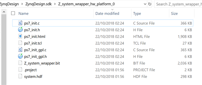
The files that are exported into the SDK/IDE can be seen using the PC’s file explorer, just for interest. The bitstream file can be seen there, as well as the various files that will allow the processor to come up and configure itself.
At this point, the developer is almost ready to start writing code! First, a board support package needs to be created which will provide the low-level functions such as the startup code (prior to running the main process) as well as basic input/output capabilities for debug using print statements to the serial console as an example. It is possible to incorporate a real-time operating system (RTOS) called FreeRTOS at this stage, but the training suggests creating the basic board support package for now.

Now that the BSP is created, the software developer can create a project and start coding.
Creating a Software Project
Much like any decent development environment for software, it is possible to use a wizard/template system to create the first project. It auto-compiles whenever it is saved.

Now I was finally ready to try it out on the real hardware : )
Running the Project
MiniZed’s boot switches were set as shown and then connected to the PC.

Using Device Manager, it was possible to see that a couple of USB Serial ports were available. One of these would be the serial console from the ARM core, but I wasn’t sure which one. I took a guess and in my case it was COM port 21. PuTTY or other serial terminal software can be used, and configured for 115200 baud with no flow control.

Next, by right-clicking on the project name in the Project Explorer pane, it was possible to select Run As -> Run Configurations and create a configuration that knew to use the USB JTAG capability to push the code into MiniZed!

The result of course was Hello World sent to the serial terminal.

The C code can now be modified as desired, and as soon as it is saved, it automatically re-compiles, and it can be executed by just clicking on the green ‘play’ icon (it will use the existing configuration to push the code to the board).

Summary
This lab exercise and hence this blog post covered a lot, but I felt it was worth it, because it really makes one feel that progress is being made. I had not thought I could get this far with Zynq so quickly to be honest.
I was pleasantly surprised. The underlying complexity in Vivado isn’t so much hidden, as actually just implemented in a way to make it easy for people to follow. This is still just beginning with Vivado, but I was very happy that these first steps are comfortably manageable even for beginners.
Thanks for following along!
Top Comments