


What is Verilog
Verilog is a Hardware Description Language (HDL). It is a language used for describing a digital system like a network switch or a microprocessor or a memory or a flip−flop. It means, by using an HDL we can describe any digital hardware at any level. Designs, which are described in HDL are independent of technology, very easy for designing and debugging, and are normally more useful than schematics, particularly for large circuits. Verilog is extensively used in FPGA development.
Verilog supports a digital design at mainly four levels of abstraction. These are −
- Behavioral level
- Register-transfer level
- Gate level
- Switch level
Behavioral level is the highest level of abstraction providel by Verilog. A module can be implemented in terms of the desired design algorithm without concern for the hardware implementation details. Designing at this level is very similar to C programming.
In gate level design the module is implemented in terms of logic gates and interconnections between these gates. Design at this level is similar to describing a design in terms of a gate-level logic diagram.
The switch level is the lowest level of abstraction provided by Verilog. A module can be implemented in terms of switches, storage nodes, and the interconnections between them. Design at this level requires knowledge of switch-level implementation details.
Verilog allows the designer to mix and match all four levels of abstractions in a design.If a design contains four modules, Verilog allows each of the modules to be written at a different level of abstraction.
Normally, the higher the level of abstraction, the more flexible and technologyindependent the design. As one goes lower toward switch-level design, the design becomes technology-dependent and inflexible. A small modification can cause a significant number of changes in the design.
In this blog post, I will try to show the design of a 4-bit full adder using Verilog and Vivado tools in multiple abstraction level. We will test the design in Cmod 7 board.
Making the Circuit
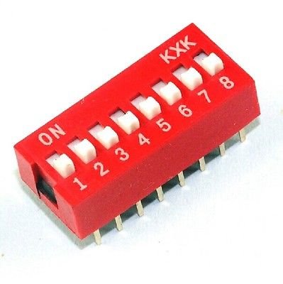
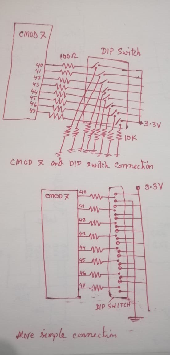
We will use a 8 bit DIP switch for providing 4-bit data to the FPGA.
The connection of the DIP switch with FPGA will be as follows:
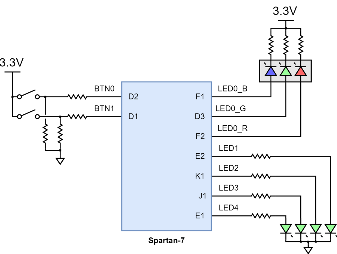
For displaying the result we will use the builtin LEDs (LED1-LED4) in the Cmod 7 board.
Verilog Code
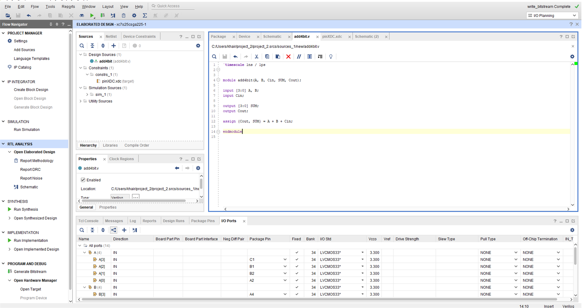
Create a new project in Vivado and create a Verilog source file named as add4bit and add the following lines of code.
Verilog code for the full adder using behavioral code:
`timescale 1ns / 1ps


module add4bit(A, B, Cin, SUM, Cout);

input [3:0] A, B;
input Cin;

output [3:0] SUM;
output Cout;

assign {Cout, SUM} = A + B + Cin;

endmodule
When programming an FPGA through software such as Xilinx's Vivado, you need to inform the software what physical pins on the FPGA that you plan on using or connecting to in relation to the HDL code that you wrote to describe the behavior of the FPGA. For example in our adder circuit we are going to use 4 leds for the output and leds are connected according to the following schematic in the Cmod 7 board.
Usually we create a hardware interface in HDL and then constrain the corresponding inputs and outputs on that interface to (essentially) whichever pins you want on the FPGA, making FPGAs very flexible for complex and custom designs.
For our connections the XDC files or constraint files is:
set_property IOSTANDARD LVCMOS33 [get_ports {A[3]}]
set_property IOSTANDARD LVCMOS33 [get_ports {A[2]}]
set_property IOSTANDARD LVCMOS33 [get_ports {A[1]}]
set_property IOSTANDARD LVCMOS33 [get_ports {A[0]}]
set_property IOSTANDARD LVCMOS33 [get_ports {B[3]}]
set_property IOSTANDARD LVCMOS33 [get_ports {B[2]}]
set_property IOSTANDARD LVCMOS33 [get_ports {B[1]}]
set_property IOSTANDARD LVCMOS33 [get_ports {B[0]}]
set_property IOSTANDARD LVCMOS33 [get_ports {SUM[3]}]
set_property IOSTANDARD LVCMOS33 [get_ports {SUM[2]}]
set_property IOSTANDARD LVCMOS33 [get_ports {SUM[1]}]
set_property IOSTANDARD LVCMOS33 [get_ports {SUM[0]}]
set_property PACKAGE_PIN A2 [get_ports {A[0]}]
set_property PACKAGE_PIN B2 [get_ports {A[1]}]
set_property PACKAGE_PIN B1 [get_ports {A[2]}]
set_property PACKAGE_PIN C1 [get_ports {A[3]}]
set_property PACKAGE_PIN B3 [get_ports {B[0]}]
set_property PACKAGE_PIN B4 [get_ports {B[1]}]
set_property PACKAGE_PIN A3 [get_ports {B[2]}]
set_property PACKAGE_PIN A4 [get_ports {B[3]}]
set_property PACKAGE_PIN E2 [get_ports {SUM[0]}]
set_property PACKAGE_PIN K1 [get_ports {SUM[1]}]
set_property PACKAGE_PIN J1 [get_ports {SUM[2]}]
set_property PACKAGE_PIN E1 [get_ports {SUM[3]}]
set_property IOSTANDARD LVCMOS33 [get_ports Cin]
set_property IOSTANDARD LVCMOS33 [get_ports Cout]
set_property PACKAGE_PIN C5 [get_ports Cin]
set_property PACKAGE_PIN F2 [get_ports Cout]
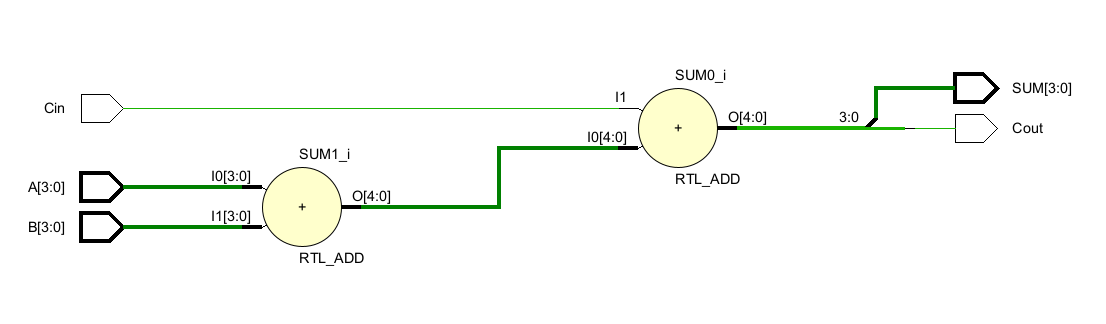
After RTL analysis of the above Verilog code we will get the following schematic.
The structural Verilog code for the full adder based on its logic diagram can be define as follows:
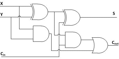
module fulladder(X, Y, Ci, S, Co);
  input X, Y, Ci;
  output S, Co;
  wire w1,w2,w3;
  //Structural code for one bit full adder
  xor G1(w1, X, Y);
  xor G2(S, w1, Ci);
  and G3(w2, w1, Ci);
  and G4(w3, X, Y);
  or G5(Co, w2, w3);
endmodule
Following is the Verilog code for the 4-bit ripple-carry adder:
module rippe_adder(X, Y, S, Co);
 input [3:0] X, Y;// Two 4-bit inputs
 output [3:0] S;
 output Co;
 wire w1, w2, w3;
 // instantiating 4 1-bit full adders in Verilog
 fulladder u1(X[0], Y[0], 1'b0, S[0], w1);
 fulladder u2(X[1], Y[1], w1, S[1], w2);
 fulladder u3(X[2], Y[2], w2, S[2], w3);
 fulladder u4(X[3], Y[3], w3, S[3], Co);
endmodule