


For making our project we need to work with images and for storing images inside an FPGA we need to use Block RAM. So, in this section, I will show how to implement Block RAM in FPGA using the Vivado tool.
What is Block RAM?
Block RAMs (or BRAM) stands for Block Random Access Memory. Block RAMs are used for storing large amounts of data efficiently inside of your FPGA like images or video, for high-performance state machines or FIFO buffer, for learge shift registers, large look up table or ROMs inside of FPGA. It is a discreate part of FPGA, meaning there are only so many of them available of them on the chip. Usually the bigger and more expensive the FPGA, the more Block RAM it will have on it. Since this is found right at the top of an FPGA product overview, it must be important! As an example, the image below shows the Product overview line comparing different Xilinx 7 series FPGAs and the Block RAM is highlighted with the blue box.

A Block RAM (sometimes called embedded memory, or Embedded Block RAM (EBR)), is a discrete part of an FPGA, meaning there are only so many of them available on the chip. Each FPGA has a different amount, so depending on your application you may need more or less Block RAM. Knowing how much you will need gets easier as you become a better Digital Designer. As I said before, it's used to store "large" amounts of data inside of your FPGA. It's also possible to store data outside of your FPGA, but that would be done with a device like an SRAM, DRAM, EPROM, SD Card, etc.
Block RAMs come in a finite size, e.g. 4/13/34 (megabits) are common in Xilinx 7 series FPGA. They have a customizable width and depth. And they're really useful for lots of applications!
When Might BRAMs be used?
- Storing large look-up tables (e.g converting celsius to fahrenheit)
- Storing read-only data such as calibration parameters
- Storing data read off external device such as ADC or Flash converter
- Creating a FIFO to store temporary data such as raw video
- Crossing clock domains using a FIFO
- In general, storing large amount of data.
A BRAM is used for storing large amount of data. A block RAM has width and depth and can be initialized to non-zero value during implimentation.

Single Port BRAM Configuration

The Single Port Block RAM configuration is useful when there is just one interface that needs to retrieve data. This is also the simplest configuration and is useful for some applications. One example would be storing Read-Only Data that is written to a fixed value when the FPGA is programmed.
The way they work is all based on a Clock. Data will be read out on the positive edge of the clock cycle at the address specified by Addr as long as Wr En signal is not active. Read values come out on Rd Data, this is the data stored in the BRAM. Note that you can only read one Rd Data value per clock cycle. So if your Block RAM is 1024 values deep, it will take at least 1024 clock cycles to read the entire thing out.
There might be an application where you want to write some data into the Block RAM buffer, then read it out at a later time. This would involve driving Wr En high for one clock cycle and Wr Data would have your write data. For the single port configuration, you can either read or write data on Port A, you can't do both at the same time. If you want to read and write data at the same time, you will need a Dual Port Block RAM!
Dual Port BRAM Configuration
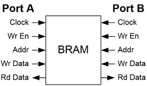
The Dual Port Block RAM (or DPRAM) configuration behaves exactly the same way as the single port configuration, except you have another port available for reading and writing data. Both Port A and Port B behave exactly the same. Port A can perform a read on Address 0 on the same clock cycle that Port B is writing to address 200. Therefore a DPRAM is able to perform a write on one address while reading from a completely different address. I personally find that I have more use cases for DPRAMs than I do for Single-Port RAMs.
One possible use case would be storing data off of an external device. For example, you want to read data off an SD Card, you could store it in a Dual Port RAM, then read it out later. Or maybe you want to interface to an Analog to Digital Converter (ADC) and will need some place to store the converted ADC values. A DPRAM would be great for this. Additionally, Dual Port RAMs are commonly turned into FIFOs, which are probably one of the most common use-cases for Block RAM on an FPGA.
How to create a Block RAM in Xilinx Vivado?
There are three different method for constructing a BRAM in Xilinx.
- Instantiation
- Inference
- IP Core
Instantiation: When we instantiate a component, we add an instance of that component to your HDL file or schematic. In a HDL file, we must use specific syntax to instantiate a component.
Inference: When we infer a component we provide a description of the function we want to accomplish. The synthesis tool then interprets the HDL code to determine which hardware components to use to perform the function.
IP Core: Xilinx provides a flexible block memory generator core to create compact, high-performance memories. The BRAM generator IP Core automates the creation of resource and power optimized block memories for Xilinx FPGAs. It result into a module that you instantiate but that does not require corresponding sourse file during synthesis. However, you must make the szource of your module available during the translate process so software tools can resolve it.
So how you want to actually create a Block RAM? Great! You have a few choices for how to proceed.
- Use Interactive GUI in Vivado. This method is easy for beginners to see how things work. This method is great to get comfortable with BRAM, but it can fall apart for large designs. The reason is that if each memory needs to be individually created, the GUI tool needs to be run many times and it becomes a burden on the FPGA designer.
- Use instantiation in VHDL or Verilog. A lot of times, you can instantiate the actual primitive for your particular FPGA. You need to refer to the Memory User's Guide for details on how this works. One nice thing about this is that you know exactly what you're getting when you directly instantiate the primitive. If you do this, it recommends writing a wrapper around it so that if you change FPGAs your main code does not have to change, just the wrapper file.
Sample BRAM implimention in Verilog
module RAM_param(clk, addr, read_write, clear, data_in, data_out);
parameter n = 4;
parameter w = 8;

input clk, read_write, clear;
input [n-1:0] addr;
input [w-1:0] data_in;
output reg [w-1:0] data_out;

// Start module here!
reg [w-1:0] reg_array [2**n-1:0];

integer i;
initial begin
    for( i = 0; i < 2**n; i = i + 1 ) begin
        reg_array[i] <= 0;
    end
end

always @(negedge(clk)) begin
    if( read_write == 1 )
        reg_array[addr] <= data_in;
    //if( clear == 1 ) begin
        //for( i = 0; i < 2**n; i = i + 1 ) begin
            //reg_array[i] <= 0;
        //end
    //end
    data_out = reg_array[addr];
end
endmodule