


If you haven't seen part 1 of the blog, do check it out!
Link: Prototyping with FPGAs - Part 1 - Basics
This blog deals with implementing a full adder on a Spartan-6 FPGA from scratch with an overview of Verilog HDL programming styles.
FPGA Design Flow:

Let's look at the first step
1. Design Entry:
FPGA Design entry can be done in two ways, either through an HDL which stands for Hardware Description Language - which is the most common method or through schematic entry wherein one can drag & drop and connect various blocks together or integrating both.
We shall discuss the design entry by exploring the Xilinx ISE!
Getting Started with Xilinx ISE:
| {gallery} ISE |
|---|
|
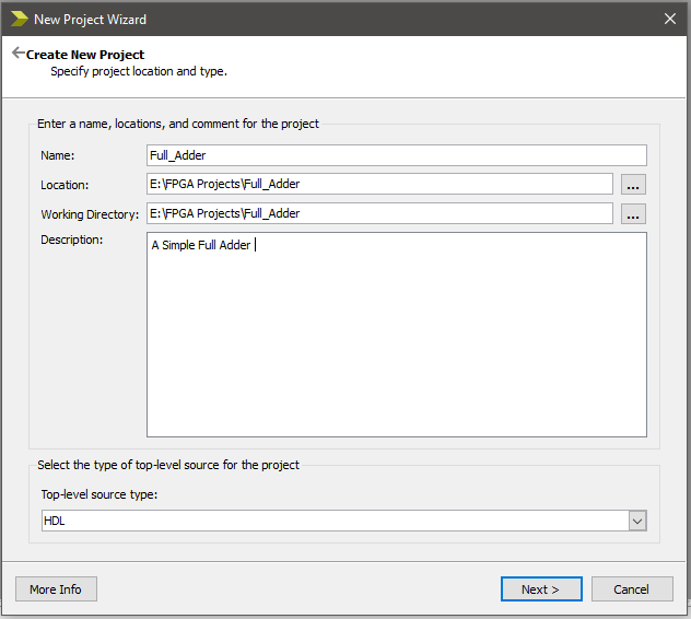
Launch ISE and create new project |
|
Name the project (spaces not preferred) and specify location |
|
Select Target device, speed grade and HDL language |
|
Finish |
|
Project created successfully. |


Full Adder Circuit (Logic):

The functionality of the circuit is pretty simple, it adds 3 bits and gives the sum and carry output.
The truth table of full adder:

What is combinational logic?
Combinational logic is a type of digital logic that is implemented by Boolean circuits, where the output is a pure function of the present input only and the circuit does not contain any memory elements.
Hardware Description Languages (HDL):
There are many HDLs out there, some of the very commonly used HDLs are Verilog, VHDL, SystemVerilog. Almost all FPGA vendors support these HDLs for synthesis.
Let's talk about Verilog in this blog. There are 3 modeling styles in Verilog.
a) Structural: Where you describe the structure of the logic circuit in terms of gates, sometimes also called Gate-level modeling.
b) Dataflow: Dataflow modeling describes hardware in terms of the flow of data from input to output.
c) Behavioural: These contain procedural statements, which control the simulation and manipulate variables of the data types.
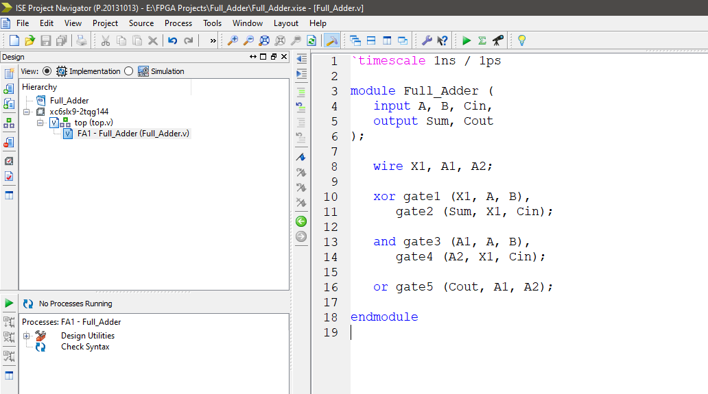
a) Full Adder Implementation using Structural modeling in Verilog:

module Full_Adder (
     input A, B, Cin,
     output Sum, Cout
);

     wire X1, A1, A2;

     xor gate1 (X1, A, B),
         gate2 (Sum, X1, Cin);

     and gate3 (A1, A, B),
         gate4 (A2, X1, Cin);

     or gate5 (Cout, A1, A2);

endmodule
b) Full Adder Implementation using dataflow modeling in Verilog:

module Full_Adder (
     input A, B, Cin,
     output Sum, Cout
);

     assign Sum = ( ( A ^ B ) ^ Cin ); // Sum = A xor B xor Cin
     assign Cout = ( ( (A ^ B) & Cin ) | ( A & B ) ); // Carry out as the equation

endmodule
c) Full Adder implementation using Behavioural modeling in Verilog:
module Full_Adder (
input A, B, Cin,
output reg Sum, Cout
);

always @ (A, B, Cin)
begin: add
     {Cout,Sum} = A + B + Cin;
end

endmodule
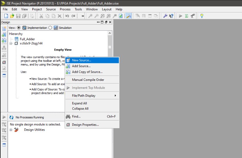
Preparing files for FPGA Design:
A typical FPGA Design would have 2 sets of files, one will have all the design files which specify the design and the other is the constraints file which will have all the constraints for the design such as the timing constraints and pin mappings for the FPGA.
It's a good practice to keep the design modular so that it's easy for development and debugging.
A top.v file (when Verilog is used as design language) is used to instantiate all the modules in a single top-level design in a Hierarchy.
| {gallery} Creating a design |
|---|
|
Add a new Source |
|
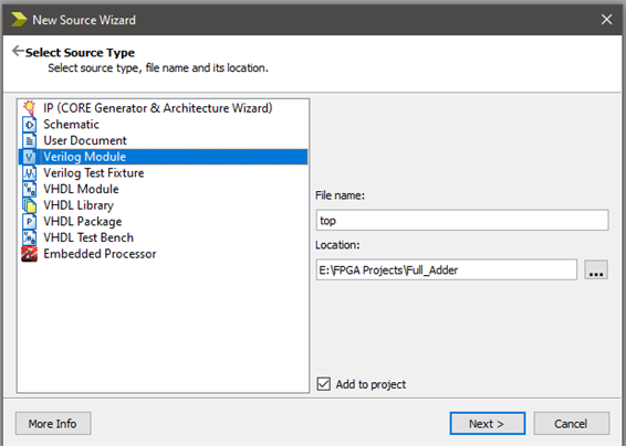
Select Verilog module and name it top |
|
Select the inputs and outputs and name them |
|
The top module will now be created |
|
Add a new source that has the code of the full adder |
|
Instantiate the full adder in the top module. |


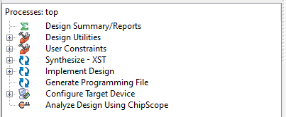
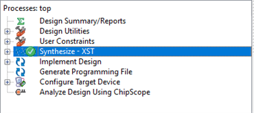
2. Design Synthesis:
During the FPGA synthesis process, a high description design or an HDL design is converted into a gate-level representation or a logic component.
Now Synthesize the design
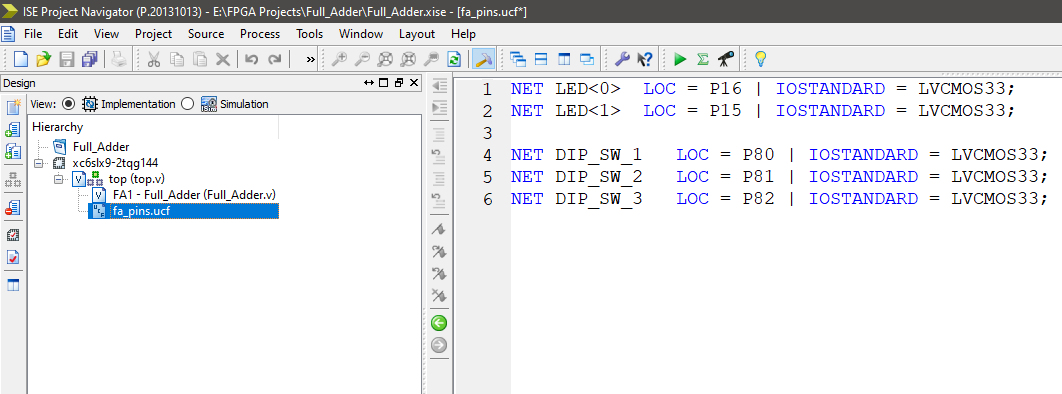
Once Synthesis is complete we need to add the constraints file to map the pins of the FPGA with the logic elements.
Create a new source and select constrains file in the options and give it a name.

Almost all the FPGA development board Vendors provide a master constrains file which contains all the pins and their mappings to the FPGA.
Copy and paste the pins that you want for your project, for instance, the 2 LEDs for Sum and Carry, then 3 switches for 3 inputs.

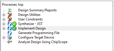
3. Design Implementation:
Now it's time to implement the design.
The Implementation tool will take the netlist as input and does optimization, placement, and routing.

4. Design Verification:

This is a simple full adder design, thus it does not require verification, yet it is a good practice to do so. The design is verified using Modelsim
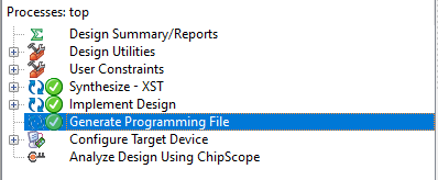
5. Generate Programming File:
The programming file is used to program the FPGA. This file contains all the information of the design implementation which is specific to an FPGA.

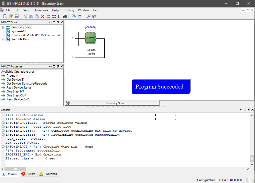
6. Programming:
Xilinx ISE has a specific tool called iMPACT which is used to program the FPGAs.

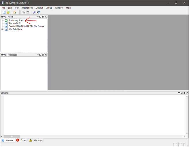
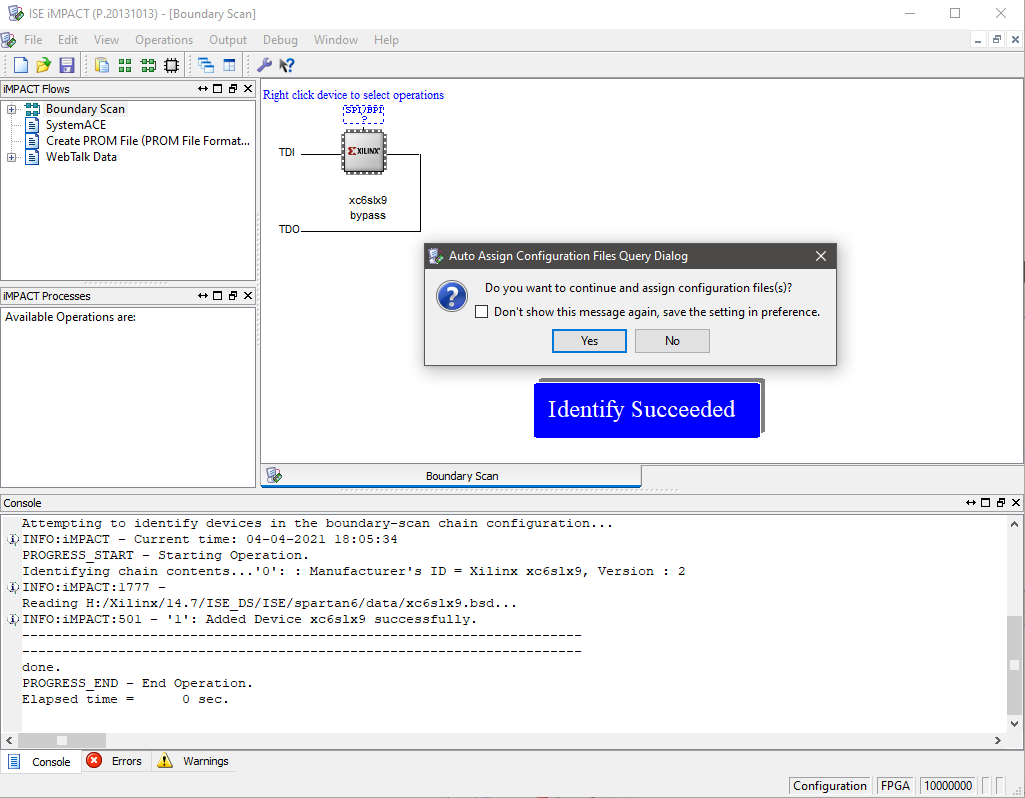
You'll get a warning asking to create an iMPACT file, click OK. Then the iMPACT tool will open, then click on Boundry Scan and then Initialize Chain.
| {gallery} My Gallery Title |
|---|
|
Click on Boundry Scan |
|
Initialize Chain |
|
|
|
Select the bit file |
|
Program the device! |
 |


Output:
Thanks for reading!
Do let me know your feedback in the comments!