


Introduction
For the past two months, I have been publishing a series of blogs introducing concepts such as Direct Digital Frequency Synthesis (DDFS), 1-bit Delta Sigma Digital to Analog Converters (DAC), and Attack, Decay, Sustain, Release (ADSR) envelope generators, with the upcoming topic of random noise generation. This project serves as a way to consolidate my initial learnings and create a small test bench for experimentation with time-based sound synthesis and noise generation.
- DDFS. Direct Digital Frequency Synthesis for Sound
- FPGA ADSR envelope generator for sound synthesis (I)
- AMD Xilinx 7 series FPGAs XADC
Music Time: Justifying the FPGA-based Music Instrument Synthesis System Design
This system designed as a test bed for the synthesis of musical instruments based on FPGA is closely linked to the concept of "musical time". Timing plays a critical role in the precise generation and synchronization of waveforms, to ensure that musical notes are played at the right time and in precise pitch.
By using the Direct Digital Synthesis (DDFS) technique, digital waveform data points are generated and converted to analog signals, which are then filtered and shaped to produce an audio output.
Additionally, the system uses techniques such as an ADSR envelope generator to shape sound waves over time, allowing for dynamic and expressive musical sounds, allowing something close to the sound of real instruments to be mimicked.
The synchronization of waveforms and effects within the FPGA enables the creation of complex audio effects or multi-timbral musical instruments, further reinforcing the close relationship between the system design and the concept of "music time".
The system
The FPGA-based music instrument synthesis system presented here can produce different types of sound waves, like sine, square, sawtooth, triangle, and noise. These waves can be changed and shaped using a technique called ADSR, which adjusts how the sound starts, fades, sustains, and stops. It uses a method called Direct Digital Synthesis (DDFS) to create these waves digitally. Then, it converts them to analog signals using a 1-bit Delta Sigma Digital to Analog Converter (DAC) and a Low Pass Filter (LPF). This allows us to have precise control over the generated sounds and mimic musical instruments and effects.
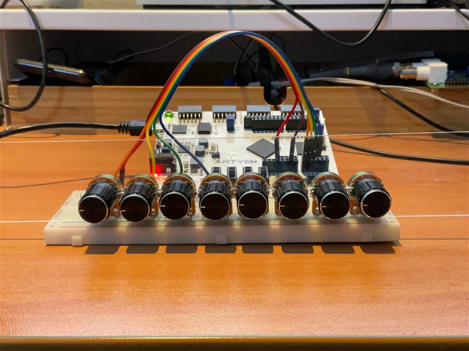
The system is based on the Digilent Arty S7 50 development board, which features an AMD Spartan-7 FPGA. It incorporates a simple RC low-pass filter and utilizes six potentiometers for parameter control. The readings from the potentiometers are captured using the XADC component from the series 7 FPGA, allowing control over the audio synthesis parameters. The audio output is connected to an amplified speaker, allowing for the synthesized sounds to be heard in real-time with amplified volume.
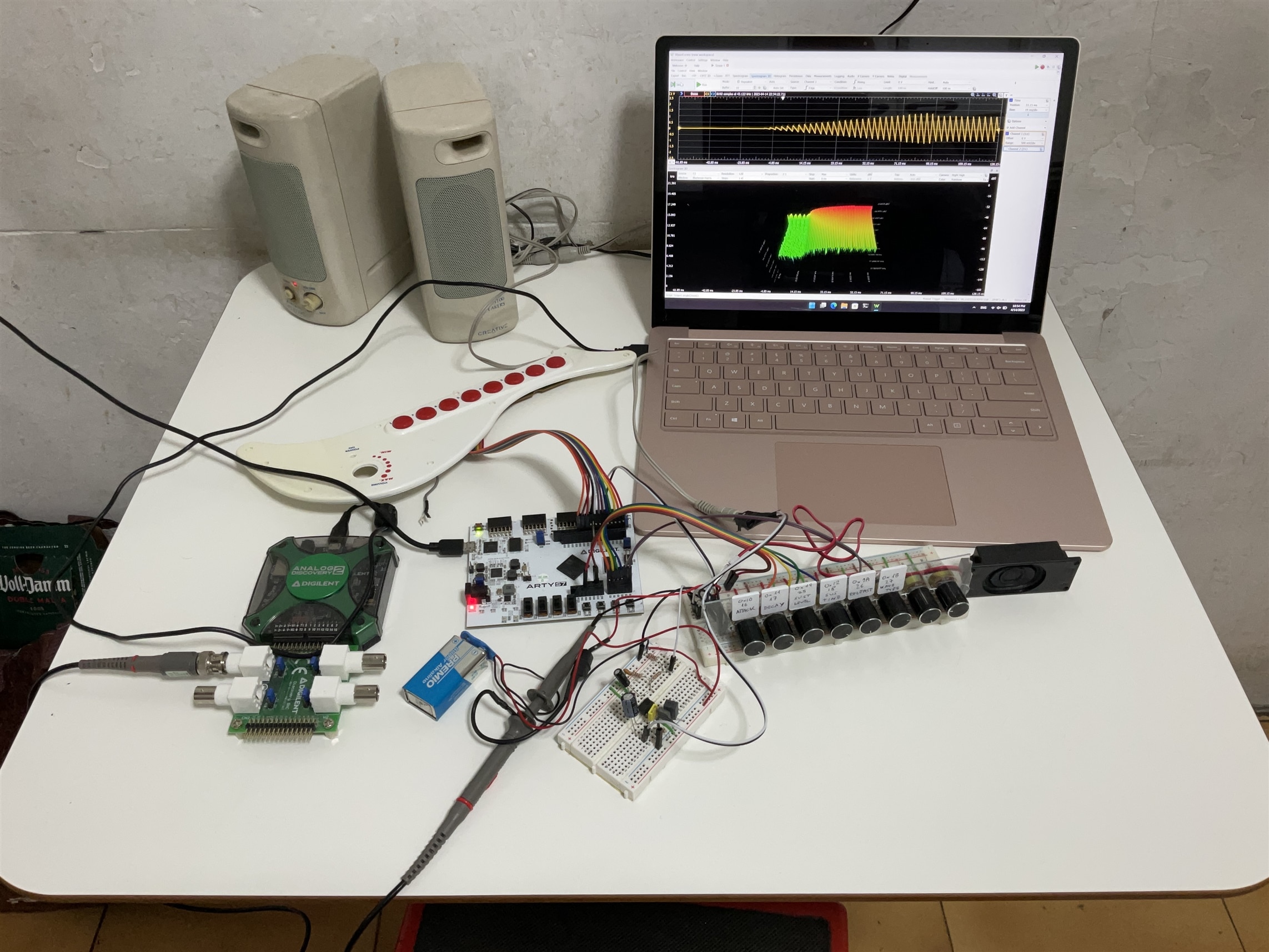
User interface
The user interface of the system consists of four buttons for selecting different notes, four slide switches for changing the octave, and six analog potentiometers for adjusting various parameters, including the ADSR parameters such as attack time, decay time, sustain level, sustain time, and release time, as well as the waveform type (such as sine, square, sawtooth, triangle, and random noise). This interface allows for control over the synthesized sounds, enabling users to shape the sound and create different musical effects.
6 analog potentiometers to control sound parameters
HDL Design
The project is heavily inspired by the book "FPGA Prototyping by SystemVerilog Examples" by Pong Chu, which has been instrumental in my introduction to FPGA hardware design using the SystemVerilog hardware description language (HDL).
All the module development in SystemVerilog, as well as the test bench for the modules and synthesis, have been carried out using the AMD Xilinx Vivado development tool.
Main Module
The main module:
- Instantiates one ILA module for debugging
- Instantiates one xadc ip module for reading the analog inputs from the Potentiometers voltage dividers
- Instantiates one ADSR module
- Instantiates one DDFS module
- Instantiates one Moving Average LPF module
- Instantiates one Delta Sigma 1-bit DAC module
- Converts 5 ADC readings to ADSR parameters for the ADSR module
- Converts 1 ADC reading to waveform type for the DDFS module
- Responds to slide switches events: changing the octave of the note frequency of the DDFS
- Respond to push button events: changing the control frequency of the DDFS
SystemVerilog implementation
`timescale 1ns / 1ps


module checkXadcAdsrNoise(
    input clk,
    input logic [3:0] sw,
    input logic [3:0] btn,
    input logic vp_in,               // input wire vp_in
    input logic vn_in,               // input wire vn_in
    input logic vauxp0,              // input wire vauxp0
    input logic vauxn0,              // input wire vauxn0
    input logic vauxp1,              // input wire vauxp1
    input logic vauxn1,              // input wire vauxn1
    input logic vauxp2,              // input wire vauxp2
    input logic vauxn2,              // input wire vauxn2
    input logic vauxp3,              // input wire vauxp3
    input logic vauxn3,              // input wire vauxn3
    input logic vauxp8,              // input wire vauxp8
    input logic vauxn8,              // input wire vauxn8
    input logic vauxp9,              // input wire vauxp9
    input logic vauxn9,              // input wire vauxn9
    input logic vauxp10,             // input wire vauxp10
    input logic vauxn10,             // input wire vauxn10
    input logic vauxp11,             // input wire vauxp11
    input logic vauxn11,             // input wire vauxn11

    output audio_out, // audio out
    output gain,      // Gain
    output pulse_out,
    output neg_shutdown, // ~SHUTDOWN
    output logic [5:0] led

    );


    localparam T = 2;
    localparam W = 16;
    localparam PHASE_ACC_WIDTH = 30;


    localparam M1 = 30'h0AFD; // (262.0 / 100_000_000.0) * (1 <<PHASE_ACC_WIDTH); // carrier freq 262 Hz Freq sys 100 Mhz, M = fout/fsys * 2^N
    localparam M2 = 30'h0C54; // (277.0 / 100_000_000.0) * (1 <<PHASE_ACC_WIDTH); // carrier freq 277 Hz Freq sys 100 Mhz, M = fout/fsys * 2^N
    localparam M3 = 30'h0DD7; // (294.0 / 100_000_000.0) * (1 <<PHASE_ACC_WIDTH); // carrier freq 294 Hz Freq sys 100 Mhz, M = fout/fsys * 2^N
    localparam M4 = 30'hEAE; // (311.0 / 100_000_000.0) * (1 <<PHASE_ACC_WIDTH); // carrier freq 311 Hz Freq sys 100 Mhz, M = fout/fsys * 2^N

    logic [31:0] attack_step_value, attack_step_value_reg   ;   // precalculated (Amax - 0)/(t_attack - t_sys) steps for the attack segment

    logic [31:0] decay_step_value, decay_step_value_reg     ;   // precalculated (A_max-A_sus) / (t_sustain / t_sys) steps for the decay segment
    logic [31:0] sustain_level, sustain_level_reg           ;   // amplitude for the sustain segment
    logic [31:0] sustain_time, sustain_time_reg             ;   // tsustain / t_sys steps for the sustain
    logic [31:0] release_step_value, release_step_value_reg ;   // precalculated (A_sus - 0)/(t_release - t_sys) steps fot the release segment"
    logic [2:0] wave_type, wave_type_reg;

    logic [15:0] adc_data;

    logic [15:0] adc0_out_reg;
    logic [15:0] adc1_out_reg;
    logic [15:0] adc2_out_reg;
    logic [15:0] adc3_out_reg;
    logic [15:0] adc4_out_reg;
    logic [15:0] adc5_out_reg;


   logic enable;
   logic ready;
   logic ready_reg;
   logic ready_rising;
   logic ready_falling;

   logic [6:0] address_in;
   logic [4:0] channel_out;
   logic eos_out;


    logic adsr_idle;
    logic   [PHASE_ACC_WIDTH-1:0] freq_carrier_ctrl_word = M1;
    logic   [PHASE_ACC_WIDTH-1:0]  freq_offset_ctrl_word = 30'h0;
    logic   [PHASE_ACC_WIDTH-1:0]  phase_offset = 30'h0;
    logic   [15:0]  amp; // = 16'h4000;  // Q2.14 format -1.0 to 1.0
    logic reset;
    logic   [PHASE_ACC_WIDTH-1:0] note;


    logic   [15:0]      pcm;                                    // pcm signal
    logic   [15:0]      pcm_lpf;                                    // pcm signal

    logic [32:0]       counter;
    logic [32:0]       counter_next;
    logic start;


       // ila instantiation
   ila_0 ila
    (   .clk,
        .probe0(adc_data),
        .probe1(channel_out),
        .probe2(enable),
        .probe3(ready),
        .probe4(eos_out)
    );


      //xadc instantiation connect the eoc_out .den_in to get continuous conversion

    xadc_adsr xadc
        (
        .daddr_in(address_in),   // Address bus for the dynamic reconfiguration port
        .dclk_in(clk),           // Clock input for the dynamic reconfiguration port
        .den_in(enable),         // Enable Signal for the dynamic reconfiguration port
        .di_in(0),               // Input data bus for the dynamic reconfiguration port
        .dwe_in(0),              // Write Enable for the dynamic reconfiguration port
        .reset_in(0),            // Reset signal for the System Monitor control logic

        .vp_in(vp_in),          // input wire vp_in
        .vn_in(vn_in),          // input wire vn_in
        .vauxp0(vauxp0),        // input wire vauxp0
        .vauxn0(vauxn0),        // input wire vauxn0
        .vauxp1(vauxp1),        // input wire vauxp1
        .vauxn1(vauxn1),        // input wire vauxn1
        .vauxp2(vauxp2),        // input wire vauxp2
        .vauxn2(vauxn2),        // input wire vauxn2
        .vauxp3(vauxp3),        // input wire vauxp3
        .vauxn3(vauxn3),        // input wire vauxn3

        .vauxp8(vauxp8),        // input wire vauxp8
        .vauxn8(vauxn8),        // input wire vauxn8
        .vauxp9(vauxp9),        // input wire vauxp9
        .vauxn9(vauxn9),        // input wire vauxn9
        .vauxp10(vauxp10),      // input wire vauxp10
        .vauxn10(vauxn10),      // input wire vauxn10
        .vauxp11(vauxp11),      // input wire vauxp11
        .vauxn11(vauxn11),      // input wire vauxn11

        .busy_out(),            // ADC Busy signal
        .channel_out(channel_out),         // Channel Selection Outputs
        .do_out(adc_data),          // Output data bus for dynamic reconfiguration port
        .drdy_out(ready),       // Data ready signal for the dynamic reconfiguration port

        .eoc_out(enable),       // End of Conversion Signal
        .eos_out(eos_out),             // End of Sequence Signal
        .alarm_out()            // OR'ed output of all the Alarms

    );

        // instantiate adsr
    adsr adsr_uut(
       .clk(clk),
       .reset(reset),
       .start(start & adsr_idle),
       .attack_step_value( attack_step_value), // precalculated (Amax - 0)/(t_attack - t_sys) steps for the attack segment
       .decay_step_value(decay_step_value),  // precalculated (A_max-A_sus) / (t_sustain / t_sys) steps for the decay segment
       .sustain_level(sustain_level), // amplitude for the sustain segment
       .release_step_value(release_step_value),  // precalculated (A_sus - 0)/(t_release - t_sys) steps fot the release segment
       .sustain_time(sustain_time), // tsustain / t_sys steps for the sustain
       .envelope(amp),
       .adsr_idle(adsr_idle)
    );


    // instantiate ddfs
    ddfs #( .PHASE_ACC_WIDTH(30)) ddfs_uut
        (.clk(clk),
        .reset(reset),
        .freq_carrier_ctrl_word(freq_carrier_ctrl_word),
        .freq_offset_ctrl_word(freq_offset_ctrl_word),
        .phase_offset(phase_offset),
        .envelope(amp),
        .pcm_out(pcm),
        .pulse_out(pulse_out),
        .wave_type(wave_type)
    );

//    moving_average_lpf lpf_uut(
//       .clk(clk),
//       .reset(reset),
//       .envelope(pcm),
//       .lpf_out(pcm_lpf)
//    );


    // instantiate ds 1bit dac
    ds_1bit_dac #(.W(16)) ds_1bit_uut(
        .clk(clk),
        .reset(reset),
        .pcm_in(pcm),
        .pdm_out(audio_out)
    );


    assign address_in = channel_out;
    assign neg_shutdown = sw[0]; // control sound on off with switch B0

    assign gain = sw[1];
    assign counter_next = counter +1;

    assign led[0] = counter[24];
    assign led[1] = pcm;

    always_ff @(posedge clk)
    begin
        ready_reg <= ready;
    end

    assign ready_rising = ready && !ready_reg ? 1'b1 : 1'b0;
    assign ready_falling = !ready && ready_reg ? 1'b1 : 1'b0;


    always_ff @(posedge clk, posedge reset)
        if (reset) begin
           attack_step_value_reg <= 32'h0000_0000;
           decay_step_value_reg <= 32'h0000_0000;
           sustain_level_reg <= 32'h0000_0000;
           sustain_time_reg <= 32'h0000_0000;
           wave_type_reg <= 3'b000;
        end else begin
        if (ready_rising == 1 && channel_out == 8'h10) begin // A1 Attack step value change
          case (adc_data[15:13])
            2:  attack_step_value_reg <= 32'h000053E3;
            3:  attack_step_value_reg <= 32'h00000863;
            4:  attack_step_value_reg <= 32'h000000D7;
            5:  attack_step_value_reg <= 32'h00000015;
            6:  attack_step_value_reg <= 32'h00000004;
            7:  attack_step_value_reg <= 32'h00000001;
            default: attack_step_value_reg <= 32'h7FFFFFFF;
          endcase
        end else begin
          attack_step_value_reg <= attack_step_value_reg;
        end

        if (ready_rising == 1 && channel_out == 8'h11) begin // A1 Decay step value change
          case (adc_data[15:13])
            2:  decay_step_value_reg <= 32'h000053E3;
            3:  decay_step_value_reg <= 32'h00000863;
            4:  decay_step_value_reg <= 32'h000000D7;
            5:  decay_step_value_reg <= 32'h00000015;
            6:  decay_step_value_reg <= 32'h00000004;
            7:  decay_step_value_reg <= 32'h00000001;
            default: decay_step_value_reg <= 32'h7FFFFFFF;
          endcase
        end else begin
          decay_step_value_reg <= decay_step_value_reg;
        end

        if (ready_rising == 1 && channel_out == 8'h19) begin // A2 Amplitude for the sustain segment value change
          case (adc_data[15:13])
            2:  sustain_level_reg <= 32'h26666666 ;
            3:  sustain_level_reg <= 32'h33333333 ;
            4:  sustain_level_reg <= 32'h40000000 ;
            5:  sustain_level_reg <= 32'h4CCCCCCC ;
            6:  sustain_level_reg <= 32'h59999999 ;
            7:  sustain_level_reg <= 32'h66666666 ;
            default: sustain_level_reg <= 32'h19999999;
          endcase
        end else begin
          sustain_level_reg <= sustain_level_reg;
        end

        if (ready_rising == 1 && channel_out == 8'h12) begin // A3 time for the sustain segment value change
          case (adc_data[15:13])
            2:  sustain_time_reg <= 32'h000186A0;
            3:  sustain_time_reg <= 32'h000F4240;
            4:  sustain_time_reg <= 32'h00989680;
            5:  sustain_time_reg <= 32'h05F5E100;
            6:  sustain_time_reg <= 32'h0DC033E0;
            7:  sustain_time_reg <= 32'h0DC1BA80;
            default: sustain_time_reg <= 32'h00000000;
          endcase
        end else begin
          sustain_time_reg <= sustain_time_reg;
        end

        if (ready_rising == 1 && channel_out == 8'h1A) begin // A4 release time for the sustain segment value change
          case (adc_data[15:13])
            2:  release_step_value_reg <= 32'h000053E3;
            3:  release_step_value_reg <= 32'h00000863;
            4:  release_step_value_reg <= 32'h000000D7;
            5:  release_step_value_reg <= 32'h00000015;
            6:  release_step_value_reg <= 32'h00000004;
            7:  release_step_value_reg <= 32'h00000001;
            default: release_step_value_reg <= 32'h7FFFFFFF;
          endcase
        end else begin
          release_step_value_reg <= release_step_value_reg;
        end

        if (ready_rising == 1 && channel_out == 8'h1B) begin // A5 wave type
          case (adc_data[15:13])
            2: wave_type_reg <= 3'b001; // saw
            3: wave_type_reg <= 3'b010; // square
            4: wave_type_reg <= 3'b011; // triangle
            5: wave_type_reg <= 3'b100; // noise
            default: wave_type_reg <= 3'b000; // sin
          endcase
        end else begin
          wave_type_reg <= wave_type_reg;
        end
    end


    assign attack_step_value  = attack_step_value_reg;   // precalculated (Amax - 0)/(t_attack - t_sys) steps for the attack segment
    assign decay_step_value   = decay_step_value_reg;   // precalculated (A_max-A_sus) / (t_sustain / t_sys) steps for the decay segment
    assign sustain_level      = sustain_level_reg;   // amplitude for the sustain segment
    assign sustain_time       = sustain_time_reg ;   // tsustain / t_sys steps for the sustain
    assign release_step_value = release_step_value_reg;  // precalculated (A_sus - 0)/(t_release - t_sys) steps fot the release segment"
    assign wave_type          = wave_type_reg;

    always_ff @(posedge clk)
    begin
        start <= btn[0] | btn[1] | btn[2] | btn[3];
        case (btn)
          4'b1000: note <= M1 << sw;
          4'b0100: note <= M2 << sw;
          4'b0010: note <= M3 << sw;
          4'b0001: note <= M4 << sw;
        endcase
    end

       // registers
   always_ff @(posedge clk, posedge reset)
   begin
      if (reset) begin
         freq_carrier_ctrl_word <= 0;
         freq_offset_ctrl_word <= 0;
         phase_offset <= 0;
         //amp <= 16'h4000;    // 1.00
         counter <=0;
      end
      else begin
            freq_carrier_ctrl_word <= note;
            freq_offset_ctrl_word <= 0;
            phase_offset <= 0;
            //amp <= 16'h4000;
            counter <= counter_next;
      end
    end

endmodule
DDFS module
Direct synthesis of a modulated analog waveform. DDFS is a digitally-controlled method of generating multiple frequencies from a reference frequency source. DDFS is a method of producing a tunable digital or analog waveform. First the data points of the waveform are generated in digital format and the converted to analog format with a Digital to Analog Converter (DAC) and a Low Pass Filter (LPF). See: One-bit Delta Sigma SystemVerilog Implementation
The DDFS module can produce five different types of waveforms: Sinusoidal, Triangle, Square, Saw-Tooth and Noise and any other wave based in Phase to Amplitude Lookup Table as waveforms captured by a microphone.
See (+) SystemVerilog Study Notes. DDFS. Direct Digital Frequency Synthesis for Sound - Blog - FPGA - element14 Community for more detail of this module
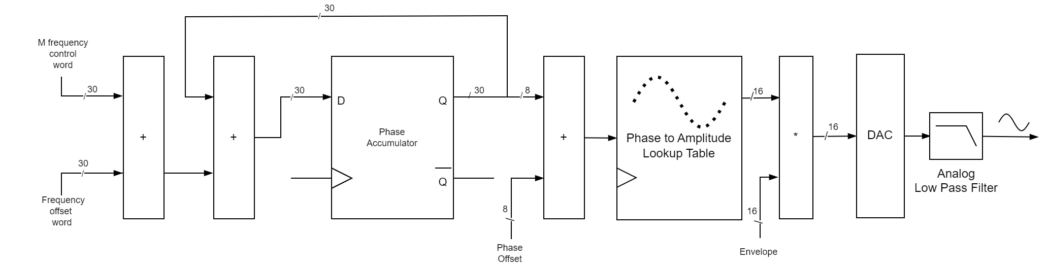
The system generates a waveform modulated this way:
modulated_wave(t) = A(t) * sin(2*PI*(f + Δf(t) * t ) + Δp(t))
- Frequency Control Word : Frequency control word (fccw) to to generate the carrier frequency
- Frequency Offset Word: The frequency control word (focw) to generate the offset frequency Δf(t)
- Phase Offset: The phase value corresponding to the desired phase offset, Δp(t)
- Envelope: The digitized value of A(t)
SystemVerilog implementation. This implementation differs from de previous one as I added four more wave types to the module
`timescale 1ns / 1ps


module ddfs
#(parameter PHASE_ACC_WIDTH = 30) // width of phase accumulator
(
    input   logic               clk,
    input   logic               reset,
    input   logic   [PHASE_ACC_WIDTH-1:0]    freq_carrier_ctrl_word,     // frequency control word to generate carrier frequency
                                                                         // fccw = fout/fsys * 2^N ; (N = PHASE_ACC_WIDTH)
    input   logic   [PHASE_ACC_WIDTH-1:0]    freq_offset_ctrl_word,      // frequency offset control word
                                                                         // focw = fout/fsys * 2^N  ; (N = PHASE_ACC_WIDTH)
    input   logic   [PHASE_ACC_WIDTH-1:0]    phase_offset,               // phase offset
                                                                         // offset/360 * 2^N ; (N = PHASE_ACC_WIDTH)
    input   logic   [15:0]      envelope,                                // Amplitude modulation: envelope, digitized value of A(t) in Q2.14 format

    input   logic   [2:0]       wave_type,                               // wave type 0 sine, 1 triangle, 2 square , 3 noise, 4 saw
    output  logic   [15:0]      pcm_out,                                 // pcm signal
    output  logic               pulse_out                                // pulse out
    );

    // signal declaration
    logic   [PHASE_ACC_WIDTH-1:0]    freq_control_word;  // frequency modulation control word
    logic   [PHASE_ACC_WIDTH-1:0]    phase_next;         // next phase
    logic   [PHASE_ACC_WIDTH-1:0]    phase_control_word; // phase control word
    logic   [PHASE_ACC_WIDTH-1:0]    phase_reg;          // actual phase
    logic   [7:0]       p2a_raddr;
    logic   [15:0]      amp;
    logic   [15:0]      sin_amp;
    logic   [15:0]      triangle_amp;
    logic   [15:0]      noise_amp;
    logic   [15:0]      square_amp;
    logic   [15:0]      saw_amp;
    logic   signed  [31:0] modulation;
    logic   [15:0] pcm_reg;  // multi-bit PCM (pulse code modulation) t
    logic   [15:0] pcm_sin_next;  // multi-bit PCM (pulse code modulation) t
    logic   [15:0] pcm_noise_next;  // multi-bit PCM (pulse code modulation) t
    logic   [15:0] pcm_square_next;  //
    logic   [15:0] pcm_triangle_next;  //
    logic   [15:0] pcm_saw_next;  //
    logic   pulse_noise;

    // body
    // instanciate sin() ROM
    sin_rom sin_rom_unit
    (   .clk(clk),
        .addr_r(p2a_raddr),
        .dout(sin_amp));

    triangle triangle_unit
    (   .clk(clk),
        .addr_r(p2a_raddr),
        .dout(triangle_amp));

    saw_tooth saw_tooth_unit
    (   .clk(clk),
        .addr_r(p2a_raddr),
        .dout(saw_amp));

    square_wave square_unit
    (   .clk(clk),
        .addr_r(p2a_raddr),
        .dout(square_amp));


    lfsr lfsr_unit(.clk(pulse_noise),
             .enable(1'b1),
             .lfsr_data(noise_amp),
             .reset(reset));

    // phase register and output buffer
    // use an output buffer (to shorten crtical path since the o/p feeds dac)
    // always_ff @(posedge clk)
    //    pcm_reg <= modu[29:14];
    always_ff @(posedge clk, posedge reset)
    begin
        if (reset)
            begin
                phase_reg <= 0;
                pcm_reg <= 0;
            end
        else
            begin
                phase_reg <= phase_next;
                pcm_reg <= pcm_next;
            end
    end

    // frequency modulation
    assign freq_control_word = freq_carrier_ctrl_word + freq_offset_ctrl_word;

    // phase accumulation
    assign phase_next = phase_reg + freq_control_word;

    assign pcm_next = modulation[29:14];

    // phase modulation
    assign phase_control_word = phase_reg + phase_offset;

    // phase to amplitude mapping address
    assign p2a_raddr = phase_control_word[PHASE_ACC_WIDTH-1:PHASE_ACC_WIDTH-8]; // 8 bits

    // amplitude modulation envelop in Q2.14
    //    * -1 < env < +1  (between 1100...00 and 0100...00)
    //    * Q16.0 * Q2.14 => modu is Q18.14
    //    * convert modu back to Q16.0

    always_comb begin
      case (wave_type[2:0])
          3'b000: amp = sin_amp;
          3'b010: amp = square_amp;
          3'b001: amp = saw_amp;
          3'b011: amp = triangle_amp;
          3'b100: amp = noise_amp;
       endcase
       modulation = $signed(envelope) * $signed(amp);
    end

    assign pcm_out = pcm_reg;
    assign pulse_out = phase_reg[PHASE_ACC_WIDTH-1];
    assign pulse_noise = phase_reg[PHASE_ACC_WIDTH-5];

endmodule
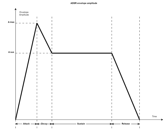
ADSR module
The ADSR scheme is based on the observation that when a real instrument generates a note, the volume of the musical note changes over time. It rises rapidly from zero and then steadily decays.
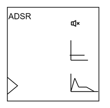
The ADSR scheme is based on the observation that when a real instrument generates a note, the volume of the musical note changes over time. It rises rapidly from zero and then steadily decays. To model this effect we can multiply the constant tone produced by the DDFS module by an amplitude ADSR envelope that contains the segments, attack, decay, sustain and release
See: (+) SystemVerilog Study Notes. FPGA ADSR envelope generator for sound synthesis (I) - Blog - FPGA - element14 Community for more info about this module
The ADRS envelope can be specified by two amplitude parameters, A max and Asus, and four time parameters, Attack time, Decay time, Sustain time and Release time.
- A max: maximum amplitude level the envelope can reach.
- A sus: the amplitude of the sustain segment.
- Attack time: the time interval of the Attack segment.
- Decay time: the time interval of the Decay segment.
- Sustain time: the time interval of the Sustain segment.
- Release time: the time interval of the Release segment.
SystemVerilog implementation.
`timescale 1ns / 1ps


// fsm to generate ADSR envelop

// start (trigger) signal:
//     - starts the "attack" when asserted
//     - restarts the epoch if aseerted before the current epoch ends

// amplitudes:
//     - 32-bit unsigned
//     - use 32 bits to accommodate the needed resolution for "step"
//     - intepreted as Q1.31 format:
//     - range artificially limited between 0.0 and 1.0
//     - i.e., 0.0...0 to 1.0...0 (1.0)
//     - 1.1xx...x not allowed

// output: Q2.14 for range (-1.0 to 1.0)

// special atk_step values
//     - atk_step = 11..11: bypass adsr; i.e., envelop=1.0
//     - atk_step = 00..00: output 0; i.e., envelop = 0.0

// Width selection:
//   max attack time = 2^31 * clock period = 2^31 *(1/100e6) = 21,47483648 seconds

// Attack_time
// t_attack desired attack time
// t_sys sytem clock period
// maximum amplitude Amax
// need t_attack / t_sys clock cycles in the attact segment
// the counter must be incremented (Amax - 0)/(t_attack - t_sys) each clock cycle to reach A_max from zero in t_attack

// Decrementing amount in decay segment for t_decay
// t_decay and A_sus.  (A_max-A_sus) / (t_sustain / t_sys)
//

// Decrementing amount in release segment
// (A_sus - 0)/(t_release - t_sys)

// The amplitude is constant in the sustain segment
// There are are tsustain / t_sys cycles in the sustain segment

// Amax  |    /\
//       |   /  \
//       |  /    \
// Asus  | /      ------------
//       |/                   \
//       ---------------------------
//        | attack
//             | decay
//                | sustain
//                            | release


 module adsr(
input logic clk,
input logic reset,
input logic start, // generate a pulse to start the envelope generation
input logic [31:0] attack_step_value, // precalculated (Amax - 0)/(t_attack - t_sys) steps for the attack segment
input logic [31:0] decay_step_value,  // precalculated (A_max-A_sus) / (t_sustain / t_sys) steps for the decay segment
input logic [31:0] sustain_level, // amplitude for the sustain segment
input logic [31:0] release_step_value,  // precalculated (A_sus - 0)/(t_release - t_sys) steps fot the release segment
input logic [31:0] sustain_time, // tsustain / t_sys steps for the sustain
output logic [15:0] envelope,
output logic adsr_idle

    );

    // constants
    localparam MAX = 32'h8000_0000;
    localparam BYPASS = 32'hffff_ffff;
    localparam ZERO = 32'h0000_0000;

    // fsm state type
    typedef enum {idle, launch, attack, decay, sustain, rel} state_type;

    // declaration
    state_type state_reg;
    state_type state_next;
    logic [31:0] amplitude_counter_reg;
    logic [31:0] amplitude_counter_next;
    logic [31:0] sustain_time_reg;
    logic [31:0] sustain_time_next;
    logic [31:0] n_tmp;
    logic fsm_idle;
    logic [31:0] envelope_i;

    // state and data registers
    always_ff @(posedge clk, posedge reset)
    begin
        if(reset)
          begin
            state_reg <= idle;
            amplitude_counter_reg <= 32'h0;
            sustain_time_reg <= 32'h0;
          end
         else
         begin
            state_reg <= state_next;
            amplitude_counter_reg <= amplitude_counter_next;
            sustain_time_reg <= sustain_time_next;
         end
    end

    // fsmd next-state logic and data path logic
    always_comb
    begin
        state_next = state_reg;
        amplitude_counter_next = amplitude_counter_reg;
        sustain_time_next = sustain_time_reg;
        fsm_idle = 1'b0;
        case (state_reg)
            idle: begin
                fsm_idle = 1'b1;
                if (start) begin
                    state_next = launch;
                  end
              end
            launch: begin
                state_next = attack;
                amplitude_counter_next = 32'b0;
              end
            attack: begin
                if(start) begin
                    state_next = launch;
                end else begin
                    n_tmp = amplitude_counter_reg + attack_step_value;
                    if (n_tmp < MAX) begin
                        amplitude_counter_next = n_tmp;
                    end else begin
                        state_next = decay;
                    end
                 end
              end
            decay: begin
                if (start) begin
                    state_next = launch;
                end else begin
                    n_tmp = amplitude_counter_reg - decay_step_value;
                    if(n_tmp > sustain_level) begin
                        amplitude_counter_next = n_tmp;
                    end else begin
                        amplitude_counter_next = sustain_level;
                        state_next = sustain;
                        sustain_time_next = 32'b0;  // start timer
                    end
                 end
              end
            sustain: begin
                if (start) begin
                    state_next = launch;
                end else begin
                    if(sustain_time_reg < sustain_time) begin
                        sustain_time_next = sustain_time_next + 1;
                    end else begin
                        state_next = rel;
                    end
                 end
              end
             default: begin
                if (start) begin
                    state_next = launch;
                  end else begin
                    if(amplitude_counter_reg > release_step_value) begin
                        amplitude_counter_next = amplitude_counter_reg - release_step_value;
                    end else begin
                        state_next = idle;
                    end
                  end
               end
        endcase

    end

    assign adsr_idle = fsm_idle;

    assign envelope_i = (attack_step_value == BYPASS) ? MAX :
                   (attack_step_value == ZERO) ? 32'b0 :
                   amplitude_counter_reg;

    assign envelope = {1'b0, envelope_i[31:17]};
endmodule
Noise Generator Module
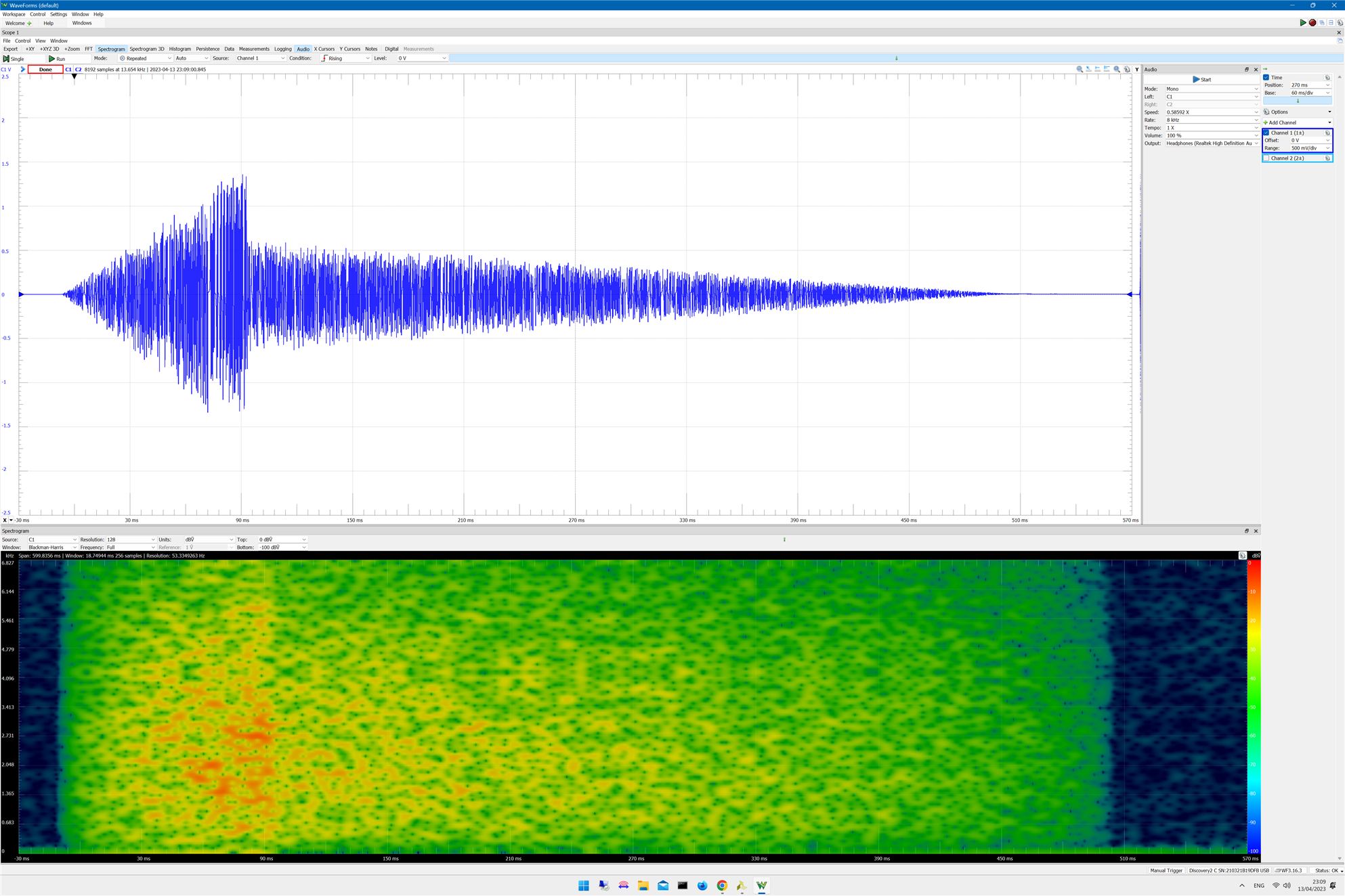
Noise is characterized as being aperiodic or having a non-repetitive pattern. White noise is a type of sound that contains all audible frequencies in equal amounts. It sounds like a hiss or a static noise. In sound synthesizers, white noise is used as a starting point for creating other sounds. By adding filters or modulating the sound, the synthesizer can create different tones or textures.
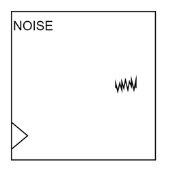
A few examples of sounds that can be created using white noise as a starting point are: the sound of a snare drum, the sound of the wind. the sound of ocean waves, the sound of cymbals...
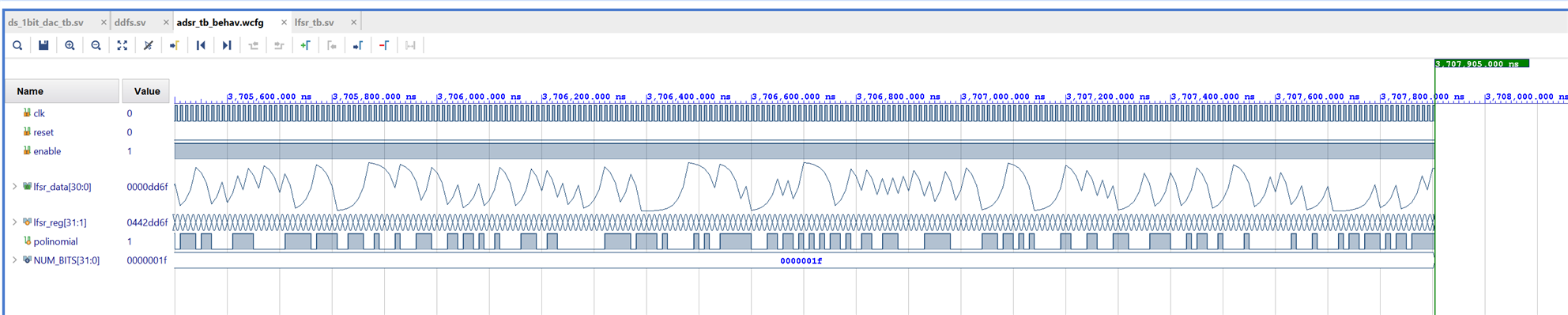
For noise generation this module uses a linear-feedback shift register (LFSR). An LFSR is a shift register whose input bit is a linear function of its previous state. The most commonly used linear function of single bits is exclusive-or (XOR). Thus, an LFSR is most often a shift register whose input bit is driven by the XOR of some bits of the overall shift register value. Any long LFSR counter generates a long pseudo-random sequence of zeros and ones. The sequence is not exactly random since it repeats eventually, and it also follows a mathematically predictable sequence.
Vivado synthesis for the SystemVerilog module
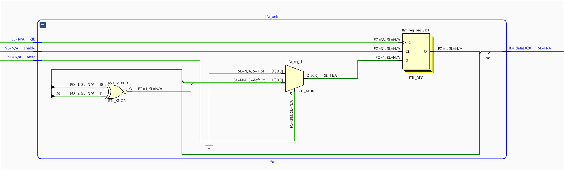
The appropriate taps for Maximum-Length LFSR Counters are extracted from this Xilinx Technical Note:
xapp052.pdf • Viewer • AMD Adaptive Computing Documentation Portal (xilinx.com)
SystemVerilog implementation of the Noise module by means of an Linear Feedback Shift Register.
`timescale 1ns / 1ps

// Description:
//  This module generates an 16-bit random number. A LFSR or Linear Feedback Shift Register
//  is a quick and easy way to generate pseudo-random data inside of an FPGA.

module lfsr #(parameter NUM_BITS = 31)
  (
   input logic clk,
   input logic reset,
   input logic enable,
   output logic [NUM_BITS-1:0] lfsr_data
   );

  logic [NUM_BITS:1] lfsr_reg = 0;
  logic polinomial;

  // run LFSR when enabled.
  always @(posedge clk, posedge reset)
    begin
      if (enable == 1'b1)
        begin
            if (reset == 1'b1) begin
                lfsr_reg <= 1'b0;
            end else begin
                lfsr_reg <= {lfsr_reg[NUM_BITS-1:1], polinomial};
            end
        end else begin
            lfsr_reg <= lfsr_reg;
        end
    end

  // Feedback Polynomial based on Xilinx Application Note:
  // http://www.xilinx.com/support/documentation/application_notes/xapp052.pdf
  // for 16 bits
  // assign  polinomial = lfsr_reg[16] ^~ lfsr_reg[15] ^~ lfsr_reg[13] ^~ lfsr_reg[4];
  // for 31 bits
   assign  polinomial = lfsr_reg[31] ^~ lfsr_reg[28];

  assign lfsr_data = lfsr_reg[16:1];

endmodule
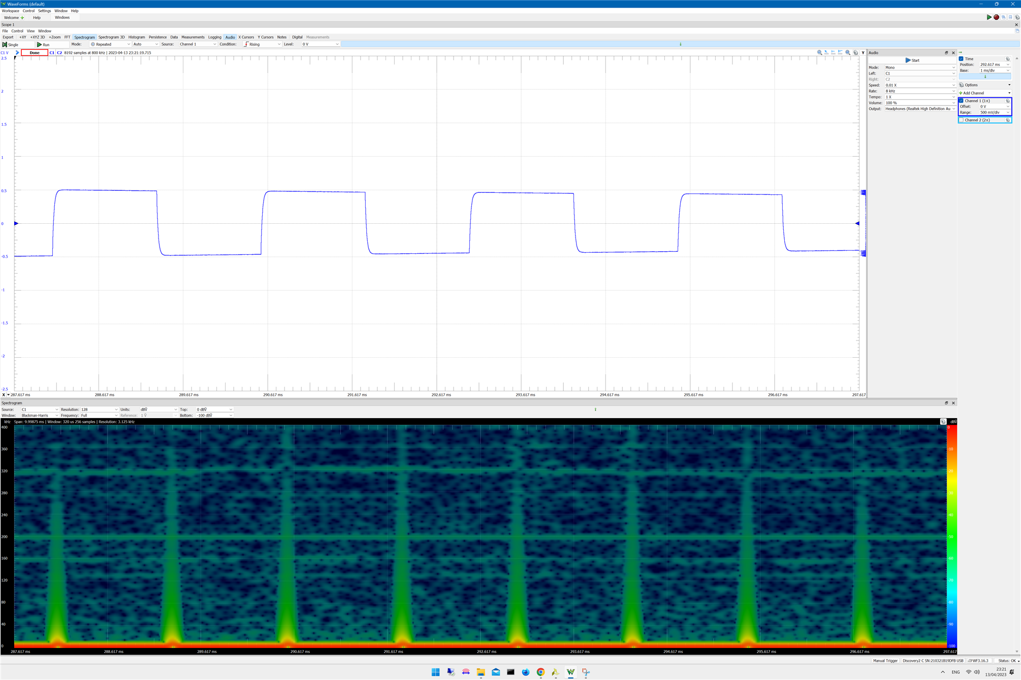
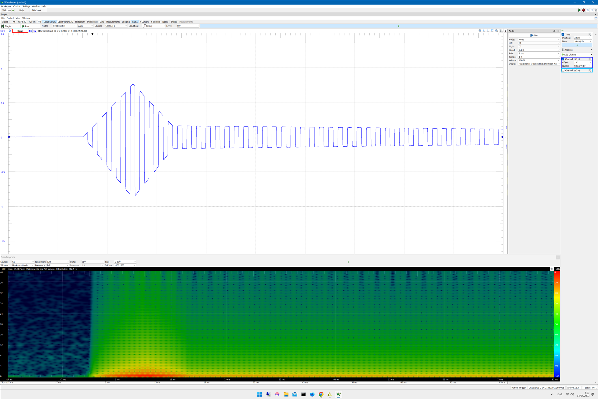
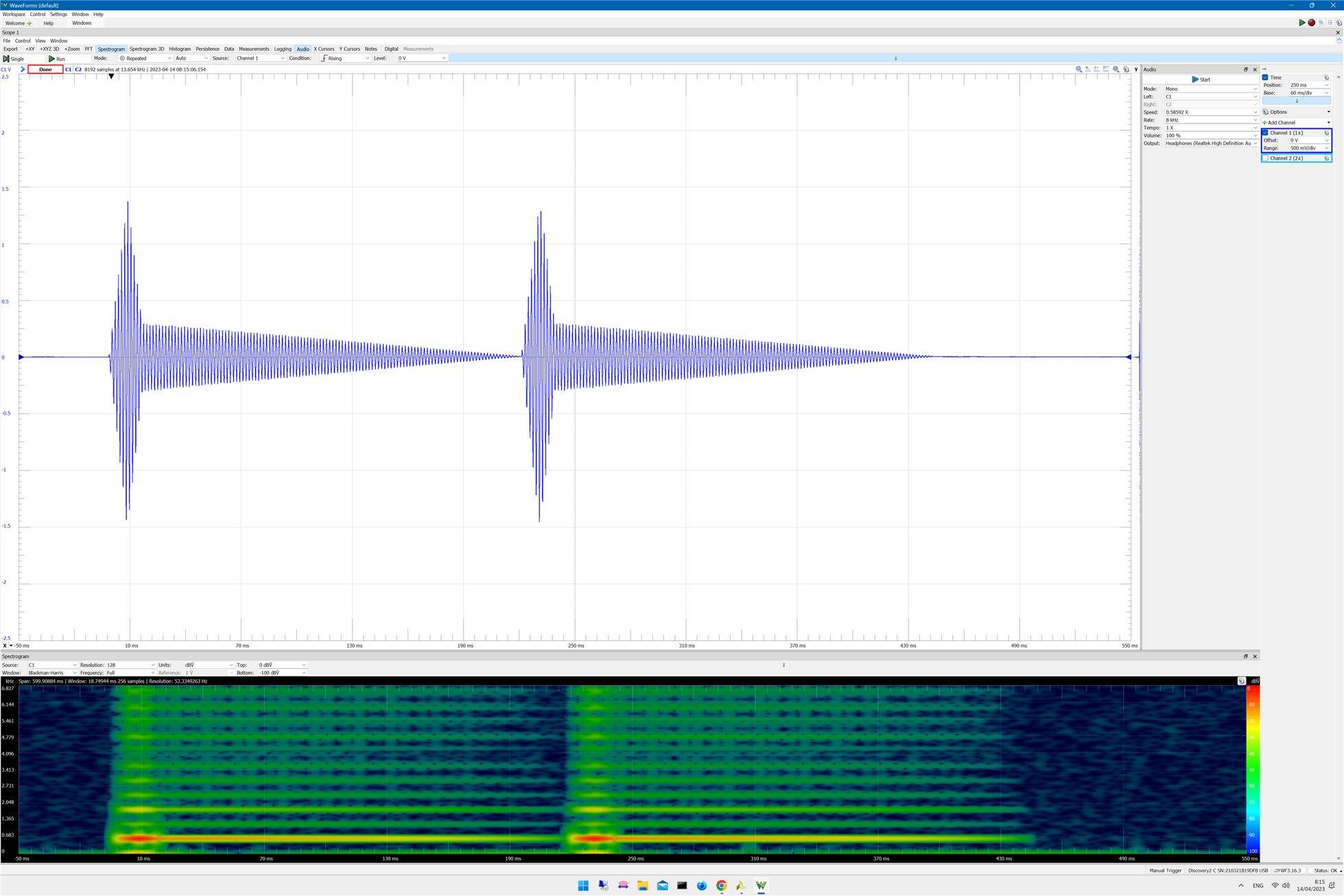
Test Bench: Synthesis Simulation in VIvado
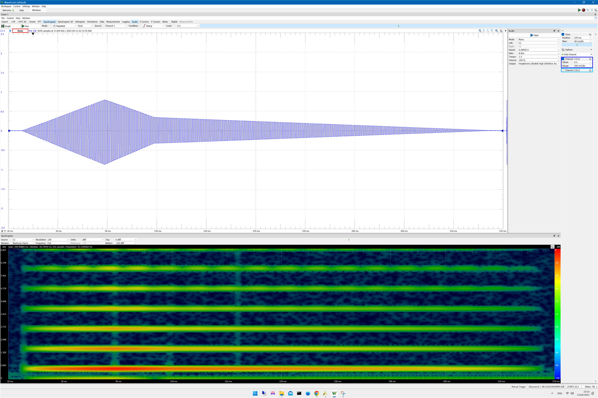
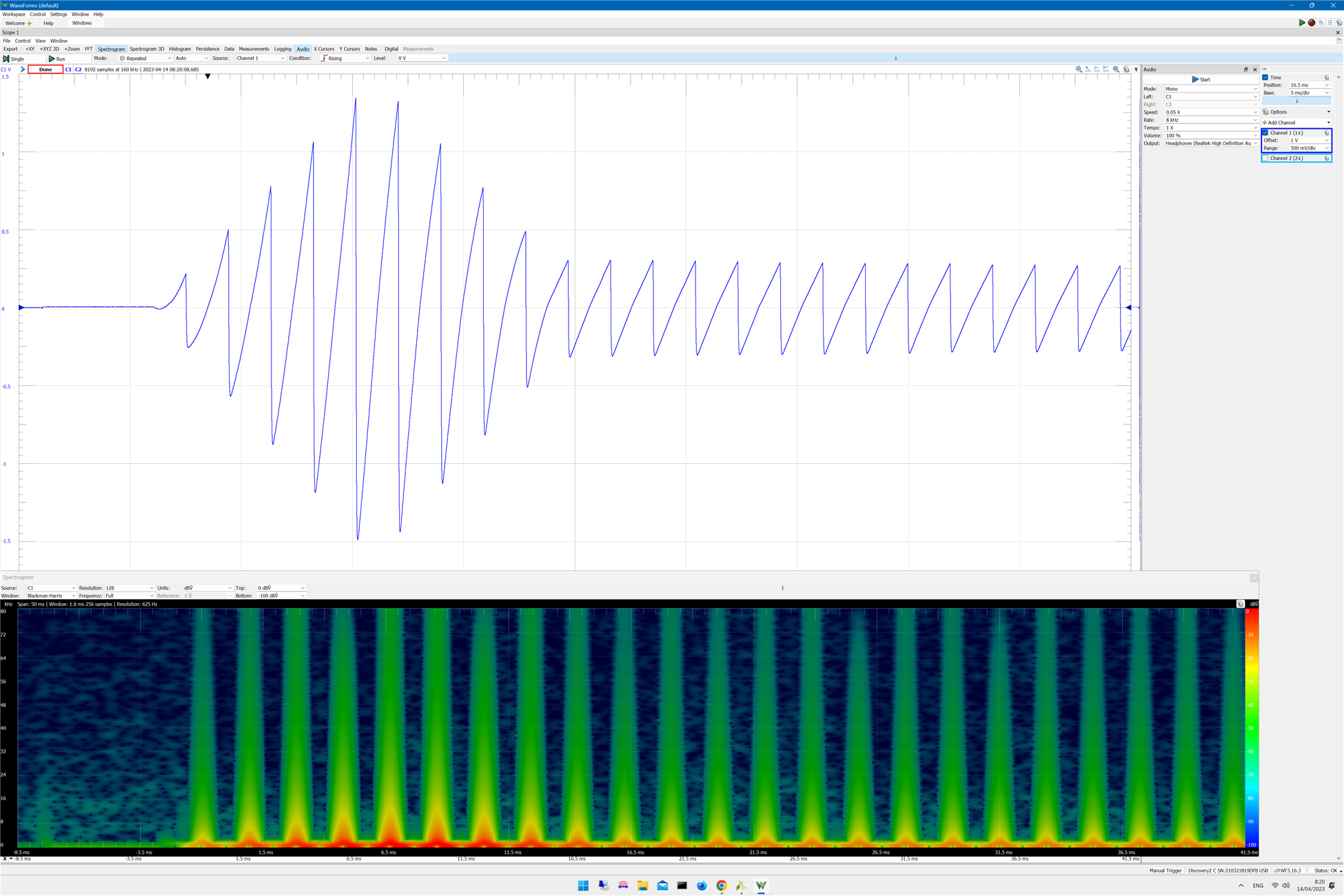
Waveform and spectrogram using noise as source
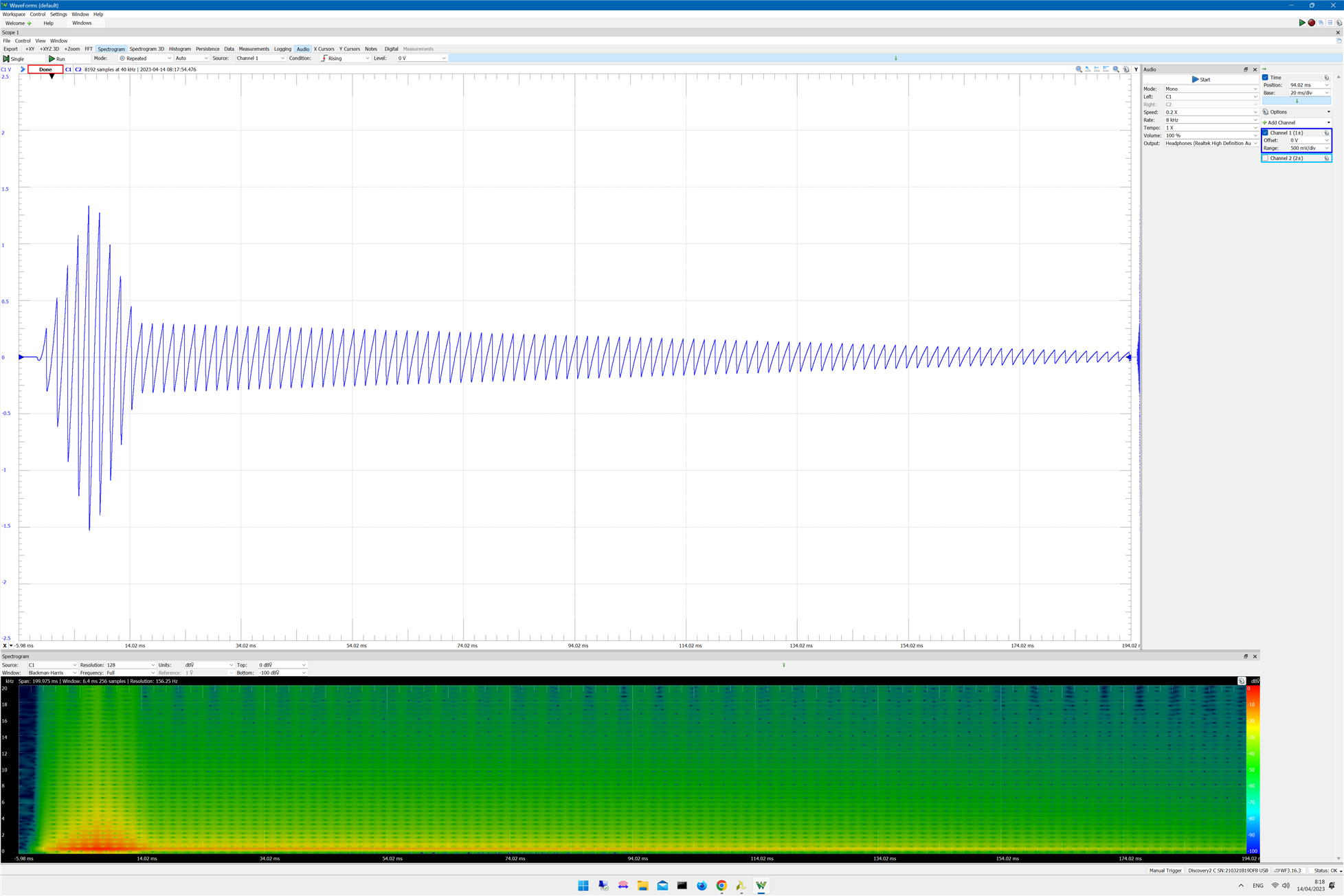
Zoomed view

Sine Wave Generator
A sine wave, sinusoidal wave, or just sinusoid is a mathematical curve defined in terms of the sine trigonometric function, of which it is the graph. It is a type of continuous wave and also a smooth periodic function. By adding different sine waves we get a different waveform, this changes the timbre of the sound. When the sound is made up of more than one sinusoidal then it has more harmonics that are perceptible to the human ear.
The presence of higher harmonics in addition to the fundamental causes variation in the timbre, which is the reason why the same musical note (the same frequency) played on different instruments sounds different. We can generate several modules with different variations in frequency and mix them.
SystemVerilog implementation
`timescale 1ns / 10ps

module sin_rom
#( parameter DATA_WIDTH = 16,  // number of bits
             ADDR_WIDTH = 8    // number od address bits

)
(
    input logic clk,
    input logic [ADDR_WIDTH-1:0] addr_r,
    output logic [DATA_WIDTH-1:0] dout
    );

    // signal declaration
    logic [DATA_WIDTH-1:0] ram [0:2**ADDR_WIDTH-1];  // ascending range
    logic [DATA_WIDTH-1:0] data_reg;

    initial
       // $readmemh("triangle_table.mem", ram);
       // $readmemh("sawtooth.mem", ram);
       $readmemh("sin_table.txt", ram);

    // read operation
    always_ff @(posedge clk)
    begin
        data_reg <= ram[addr_r];
    end

    assign dout = data_reg;
endmodule
Waveform and spectrogram using one sin module as source
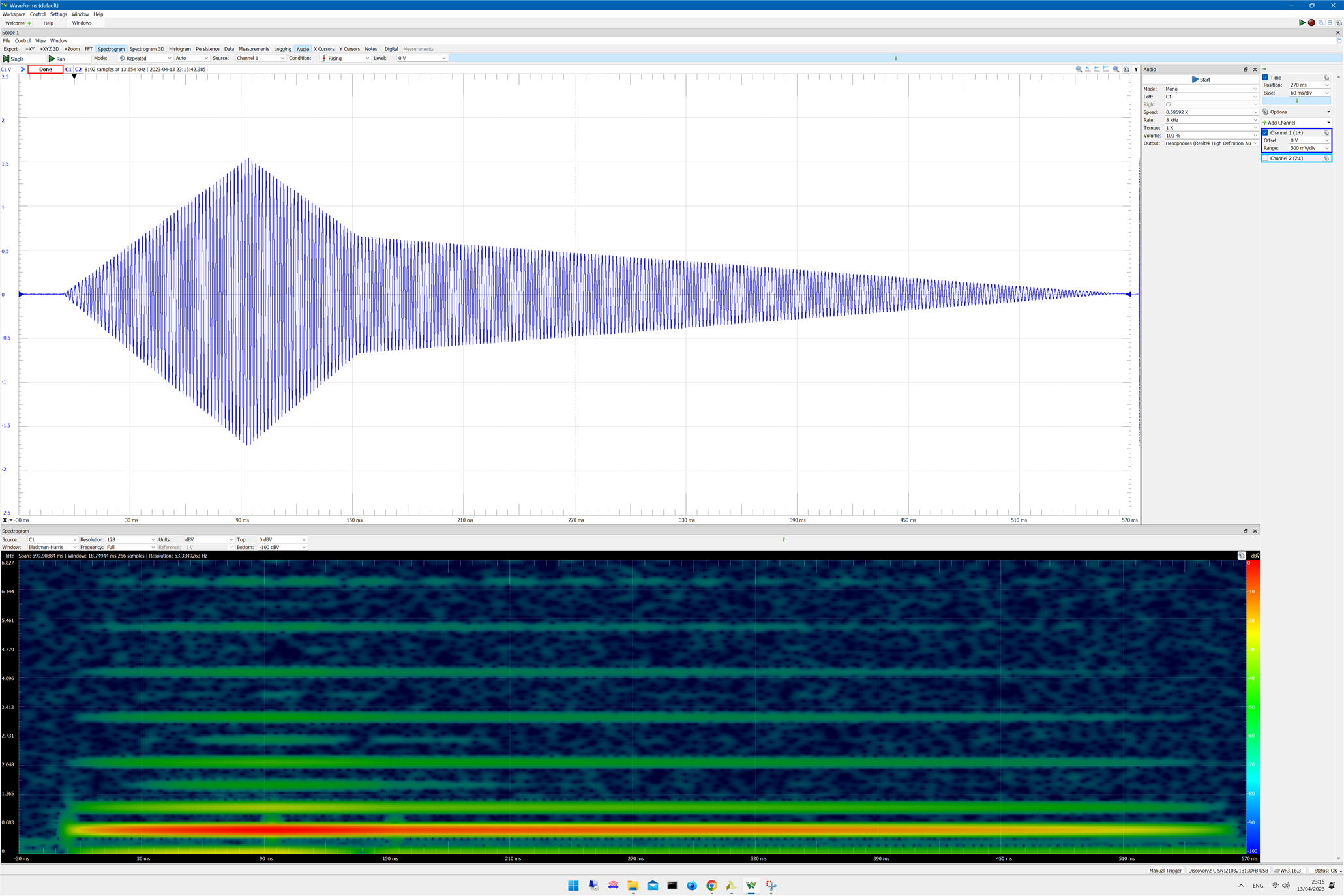
Zoomed view:

Square Wave Generator
A square wave is a non-sinusoidal periodic waveform in which the amplitude alternates at a steady frequency between fixed minimum and maximum values, with the same duration at minimum and maximum. In an ideal square wave, the transitions between minimum and maximum are instantaneous, Square waves contain a wide range of harmonics. The ideal square wave contains only components of odd-integer harmonic frequencies.
In music they are described as hollow sounds. They can be used as the basis for wind instrument sounds created using subtractive synthesis.
Also for performing distortion effects by clipping the outermost regions of the waveform, making it more and more like a square wave as more distortion is applied.
SystemVerilog implementation for the square wave generator.
`timescale 1ns / 1ps

/**
A square wave is a non-sinusoidal periodic waveform
in which the amplitude alternates at a steady frequency between
fixed minimum and maximum values, with the same duration at minimum and maximum.
n musical terms, they are often described as sounding hollow, and are therefore
used as the basis for wind instrument sounds created using subtractive synthesis.
Additionally, the distortion effect used on electric guitars clips the outermost
regions of the waveform, causing it to increasingly resemble
a square wave as more distortion is applied.
*/
module square_wave
#( parameter DATA_WIDTH = 16,  // number of bits
             ADDR_WIDTH = 8    // number od address bits

)
(
    input logic clk,
    input logic [ADDR_WIDTH-1:0] addr_r,
    output logic [DATA_WIDTH-1:0] dout
    );

    // signal declaration
    logic [DATA_WIDTH-1:0] data_reg;
    logic [DATA_WIDTH-1:0] data;


    // read operation
    always_ff @(posedge clk)
    begin
        data_reg <= data;
    end

    always_comb
    begin
       data = addr_r[7]?16'b1100_0000_0000_0000:16'b0100_0000_0000_0000;
    end

    assign dout = data_reg;
endmodule
Waveform and spectrogram using one square module as source
Zoomed view
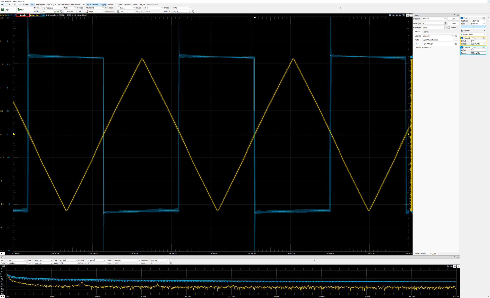
Triangle Wave Generator
A triangular wave or triangle wave is a non-sinusoidal waveform named for its triangular shape. It is a periodic, piecewise linear, continuous real function. Like a square wave, the triangle wave contains only odd harmonics. However, the higher harmonics roll off much faster than in a square wave (proportional to the inverse square of the harmonic number as opposed to just the inverse).
ROM look-up table based SystemVerilog Implementation
`timescale 1ns / 10ps

module triangle_rom
#( parameter DATA_WIDTH = 16,  // number of bits
             ADDR_WIDTH = 8    // number od address bits

)
(
    input logic clk,
    input logic [ADDR_WIDTH-1:0] addr_r,
    output logic [DATA_WIDTH-1:0] dout
    );

    // signal declaration
    logic [DATA_WIDTH-1:0] ram [0:2**ADDR_WIDTH-1];  // ascending range
    logic [DATA_WIDTH-1:0] data_reg;

    initial
        $readmemh("triangle_table.mem", ram);
     //  $readmemh("sawtooth.mem", ram);
     //  $readmemh("triangle_table.txt", ram);

    // read operation
    always_ff @(posedge clk)
    begin
        data_reg <= ram[addr_r];
    end

    assign dout = data_reg;
endmodule
Triangle Wave Generator from Equations
`timescale 1ns / 10ps

/**
A triangular wave or triangle wave is a non-sinusoidal waveform
named for its triangular shape. It is a periodic, piecewise linear,
continuous real function. Like a square wave, the triangle wave
contains only odd harmonics.
The higher harmonics roll off much faster than in a square wave.
*/

module triangle
#( parameter DATA_WIDTH = 16,  // number of bits
             ADDR_WIDTH = 8    // number od address bits

)
(
    input logic clk,
    input logic [ADDR_WIDTH-1:0] addr_r,
    output logic [DATA_WIDTH-1:0] dout
    );

    // signal declaration
    logic [DATA_WIDTH-1:0] data_reg;
    logic [DATA_WIDTH-1:0] data;

    // read operation
    always_ff @(posedge clk)
    begin
        data_reg <= data;
    end

    always_comb
    begin
      if (addr_r > 8'h7F) begin
           data = {8'h00, 8'hFE - addr_r}; // decaying
      end else begin
           data = {8'h00, addr_r}; // raising
      end
    end

    assign dout =  $signed(data << 9) - $signed(16'h8000);  // offset biass
endmodule
Saw-Tooth Generator Module
Sawtooth waves and real-world signals contain all integer harmonics.
`timescale 1ns / 10ps


module saw_tooth
#( parameter DATA_WIDTH = 16,  // number of bits
             ADDR_WIDTH = 8    // number od address bits

)
(
    input logic clk,
    input logic [ADDR_WIDTH-1:0] addr_r,
    output logic [DATA_WIDTH-1:0] dout
    );

    // signal declaration
    logic [DATA_WIDTH-1:0] data_reg;
    logic [DATA_WIDTH-1:0] data;
    logic [DATA_WIDTH-1:0] amp;


    // read operation
    always_ff @(posedge clk)
    begin
        data_reg <= data;
    end


    always_comb
    begin
      amp = {8'h00, addr_r} << 8;
      data = $signed(amp) - $signed(16'h8000);
    end


    assign dout = data_reg;
endmodule
XADC Sequencer Mode
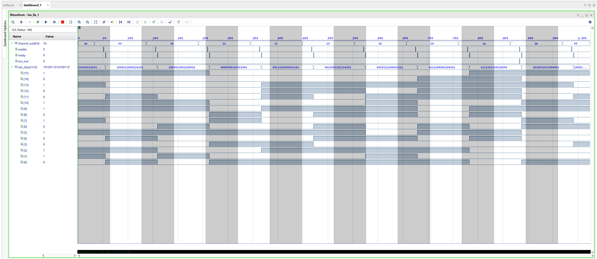
The reading of the potentiometers to control the attack time, the decay time, the sustain amplitude value, the sustain time and the release time of the ADSR module as well as the type of wave to be generated is done with the XADC module of the AMD Spartan 7 FPGA configured in sequencer mode, gives us the readings of the six potentiometers in sequence. See the ILA capture, when the ready signal is asserted we can read the value corresponding to the active sequence channel.
Verilog XADC configuration module
`timescale 1ns / 1 ps

(* CORE_GENERATION_INFO = "xadc_adsr,xadc_wiz_v3_3_8,
{component_name=xadc_adsr,
enable_axi=false,
enable_axi4stream=false,
dclk_frequency=100,
enable_busy=true,
enable_convst=false,
enable_convstclk=false,
enable_dclk=true,
enable_drp=true,
enable_eoc=true,
enable_eos=true,
enable_vbram_alaram=false,
enable_vccddro_alaram=false,
enable_Vccint_Alaram=false,
enable_Vccaux_alaram=false,
enable_vccpaux_alaram=false,
enable_vccpint_alaram=false,
ot_alaram=false,
user_temp_alaram=false,
timing_mode=continuous,
channel_averaging=None,
sequencer_mode=on,
startup_channel_selection=contineous_sequence}" *)


module xadc_adsr
          (
          daddr_in,            // Address bus for the dynamic reconfiguration port
          dclk_in,             // Clock input for the dynamic reconfiguration port
          den_in,              // Enable Signal for the dynamic reconfiguration port
          di_in,               // Input data bus for the dynamic reconfiguration port
          dwe_in,              // Write Enable for the dynamic reconfiguration port
          reset_in,            // Reset signal for the System Monitor control logic
          vauxp0,              // Auxiliary channel 0
          vauxn0,
          vauxp1,              // Auxiliary channel 1
          vauxn1,
          vauxp2,              // Auxiliary channel 2
          vauxn2,
          vauxp3,              // Auxiliary channel 3
          vauxn3,
          vauxp8,              // Auxiliary channel 8
          vauxn8,
          vauxp9,              // Auxiliary channel 9
          vauxn9,
          vauxp10,             // Auxiliary channel 10
          vauxn10,
          vauxp11,             // Auxiliary channel 11
          vauxn11,
          busy_out,            // ADC Busy signal
          channel_out,         // Channel Selection Outputs
          do_out,              // Output data bus for dynamic reconfiguration port
          drdy_out,            // Data ready signal for the dynamic reconfiguration port
          eoc_out,             // End of Conversion Signal
          eos_out,             // End of Sequence Signal
          alarm_out,           // OR'ed output of all the Alarms
          vp_in,               // Dedicated Analog Input Pair
          vn_in);

          input [6:0] daddr_in;
          input dclk_in;
          input den_in;
          input [15:0] di_in;
          input dwe_in;
          input reset_in;
          input vauxp0;
          input vauxn0;
          input vauxp1;
          input vauxn1;
          input vauxp2;
          input vauxn2;
          input vauxp3;
          input vauxn3;
          input vauxp8;
          input vauxn8;
          input vauxp9;
          input vauxn9;
          input vauxp10;
          input vauxn10;
          input vauxp11;
          input vauxn11;
          input vp_in;
          input vn_in;

          output busy_out;
          output [4:0] channel_out;
          output [15:0] do_out;
          output drdy_out;
          output eoc_out;
          output eos_out;
          output alarm_out;

        wire FLOAT_VCCAUX;
        wire FLOAT_VCCINT;
        wire FLOAT_TEMP;
          wire GND_BIT;
    wire [2:0] GND_BUS3;
          assign GND_BIT = 0;
    assign GND_BUS3 = 3'b000;
          wire [15:0] aux_channel_p;
          wire [15:0] aux_channel_n;
          wire [7:0]  alm_int;
          assign alarm_out = alm_int[7];
          assign aux_channel_p[0] = vauxp0;
          assign aux_channel_n[0] = vauxn0;

          assign aux_channel_p[1] = vauxp1;
          assign aux_channel_n[1] = vauxn1;

          assign aux_channel_p[2] = vauxp2;
          assign aux_channel_n[2] = vauxn2;

          assign aux_channel_p[3] = vauxp3;
          assign aux_channel_n[3] = vauxn3;

          assign aux_channel_p[4] = 1'b0;
          assign aux_channel_n[4] = 1'b0;

          assign aux_channel_p[5] = 1'b0;
          assign aux_channel_n[5] = 1'b0;

          assign aux_channel_p[6] = 1'b0;
          assign aux_channel_n[6] = 1'b0;

          assign aux_channel_p[7] = 1'b0;
          assign aux_channel_n[7] = 1'b0;

          assign aux_channel_p[8] = vauxp8;
          assign aux_channel_n[8] = vauxn8;

          assign aux_channel_p[9] = vauxp9;
          assign aux_channel_n[9] = vauxn9;

          assign aux_channel_p[10] = vauxp10;
          assign aux_channel_n[10] = vauxn10;

          assign aux_channel_p[11] = vauxp11;
          assign aux_channel_n[11] = vauxn11;

          assign aux_channel_p[12] = 1'b0;
          assign aux_channel_n[12] = 1'b0;

          assign aux_channel_p[13] = 1'b0;
          assign aux_channel_n[13] = 1'b0;

          assign aux_channel_p[14] = 1'b0;
          assign aux_channel_n[14] = 1'b0;

          assign aux_channel_p[15] = 1'b0;
          assign aux_channel_n[15] = 1'b0;
XADC #(
        .INIT_40(16'h0000), // config reg 0
        .INIT_41(16'h21AF), // config reg 1
        .INIT_42(16'h0400), // config reg 2
        .INIT_48(16'h0800), // Sequencer channel selection
        .INIT_49(16'h0F0F), // Sequencer channel selection
        .INIT_4A(16'h0000), // Sequencer Average selection
        .INIT_4B(16'h0000), // Sequencer Average selection
        .INIT_4C(16'h0000), // Sequencer Bipolar selection
        .INIT_4D(16'h0000), // Sequencer Bipolar selection
        .INIT_4E(16'h0000), // Sequencer Acq time selection
        .INIT_4F(16'h0000), // Sequencer Acq time selection
        .INIT_50(16'hB5ED), // Temp alarm trigger
        .INIT_51(16'h57E4), // Vccint upper alarm limit
        .INIT_52(16'hA147), // Vccaux upper alarm limit
        .INIT_53(16'hCA33),  // Temp alarm OT upper
        .INIT_54(16'hA93A), // Temp alarm reset
        .INIT_55(16'h52C6), // Vccint lower alarm limit
        .INIT_56(16'h9555), // Vccaux lower alarm limit
        .INIT_57(16'hAE4E),  // Temp alarm OT reset
        .INIT_58(16'h5999), // VCCBRAM upper alarm limit
        .INIT_5C(16'h5111),  //  VCCBRAM lower alarm limit
        .SIM_DEVICE("7SERIES"),
        .SIM_MONITOR_FILE("design.txt")
)

inst (
        .CONVST(GND_BIT),
        .CONVSTCLK(GND_BIT),
        .DADDR(daddr_in[6:0]),
        .DCLK(dclk_in),
        .DEN(den_in),
        .DI(di_in[15:0]),
        .DWE(dwe_in),
        .RESET(reset_in),
        .VAUXN(aux_channel_n[15:0]),
        .VAUXP(aux_channel_p[15:0]),
        .ALM(alm_int),
        .BUSY(busy_out),
        .CHANNEL(channel_out[4:0]),
        .DO(do_out[15:0]),
        .DRDY(drdy_out),
        .EOC(eoc_out),
        .EOS(eos_out),
        .JTAGBUSY(),
        .JTAGLOCKED(),
        .JTAGMODIFIED(),
        .OT(),
        .MUXADDR(),
        .VP(vp_in),
        .VN(vn_in)
          );

endmodule
Moving Average LPF
Another design of mine for a configurable low pass filter based on a moving average that hardly uses FPGA resources.
`timescale 1ns / 1ps
///////////////////////////////////////////////////////////////////////


module moving_average_lpf(
    input logic clk,
    input logic reset,
    output logic [15:0] envelope,
    output logic [15:0] lpf_out
);

    logic [31:0] ma_new, ma_new_reg;
    logic [31:0] ma_old, ma_old_reg;
    logic [31:0] envelope_i;


    always_ff @(posedge clk, posedge reset) begin
        if (reset) begin
            ma_new_reg <=0;
            ma_old_reg <=0;
        end else begin
            ma_new_reg <= ma_new;
            ma_old_reg <= ma_old;
        end
    end
    assign envelope_i = {envelope[14:0] , 17'b0};
    assign ma_old = ma_new_reg;
    assign ma_new = ( envelope_i  >> 17) + (ma_old_reg - (ma_old_reg >> 17)) ;

    assign lpf_out =  {1'b0, ma_new_reg[31:17]};

endmodule
Echo Delay
Still in development this is the first version to implement an echo or feedback delay module.
`timescale 1ns / 1ps

module echo #(DELAY_LINE_SIZE = 1024)(
  input logic clk,
  input logic reset,
  input logic [15:0] in,
  input logic [7:0] delay,
  input logic [7:0] feedback,
  output logic [15:0] out
);


  logic [15:0] delay_line [DELAY_LINE_SIZE];
  int write_ptr = 0, read_ptr = 0;
  logic [15:0] echo_signal;

  always_ff @(posedge clk, posedge reset) begin
    if(reset) begin
        write_ptr = 0;
        read_ptr = 0;
    end else begin
      // Write input to delay line and compute echo signal
      delay_line[write_ptr] = in;
      echo_signal = delay_line[read_ptr] * feedback;
      read_ptr = (read_ptr + delay) % DELAY_LINE_SIZE;
      write_ptr = (write_ptr + 1) % DELAY_LINE_SIZE;
      // Mix input and echo signals
      out = in + echo_signal;
    end
  end

endmodule
HDL Sources
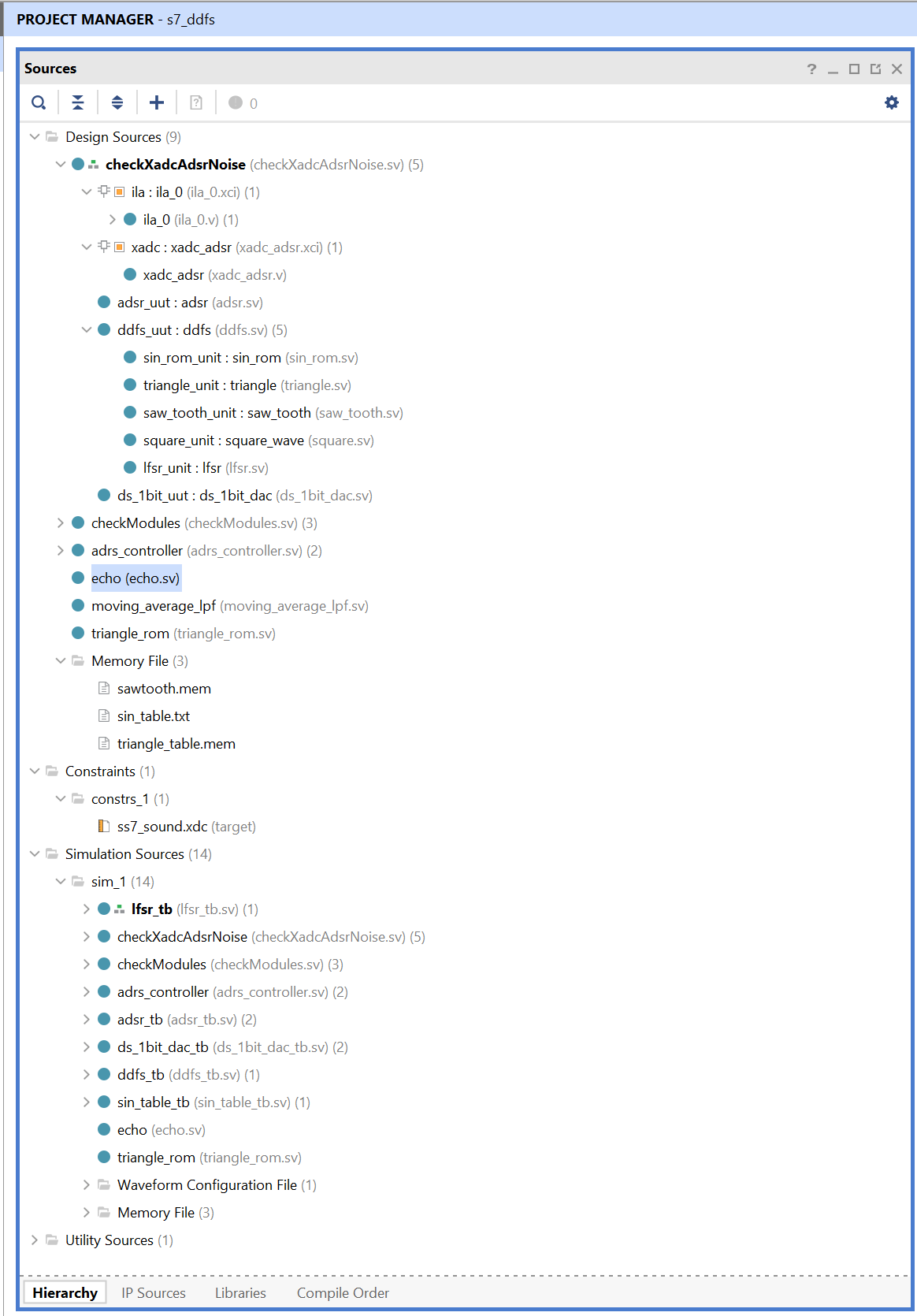
Vivado Project Structure
The project contains all the modules indicated in the blog as well as test bench modules for simulations.
Constraints File
This constraints file is adapted to the current system configuration, 4 monocolor LEDs, 2 RGB LEDs, 4 slide switches, 4 push buttons, 6 analog potentiometers used with the XADC module of the Spartan 7 FPGA and the PDM digital output to the RC low-pass analog filter. .
## This file is a general .xdc for the Arty S7-50 Rev. B

## Clock Signals
set_property -dict {PACKAGE_PIN R2 IOSTANDARD SSTL135} [get_ports clk]
create_clock -period 10.000 -name sys_clk_pin -waveform {0.000 5.000} -add [get_ports clk]

## Switches
set_property -dict {PACKAGE_PIN H14 IOSTANDARD LVCMOS33} [get_ports {sw[0]}]
set_property -dict {PACKAGE_PIN H18 IOSTANDARD LVCMOS33} [get_ports {sw[1]}]
set_property -dict {PACKAGE_PIN G18 IOSTANDARD LVCMOS33} [get_ports {sw[2]}]
set_property -dict {PACKAGE_PIN M5 IOSTANDARD SSTL135} [get_ports {sw[3]}]

## LEDs
set_property -dict {PACKAGE_PIN E18 IOSTANDARD LVCMOS33} [get_ports {led[0]}]
set_property -dict {PACKAGE_PIN F13 IOSTANDARD LVCMOS33} [get_ports {led[1]}]
set_property -dict {PACKAGE_PIN E13 IOSTANDARD LVCMOS33} [get_ports {led[2]}]
set_property -dict {PACKAGE_PIN H15 IOSTANDARD LVCMOS33} [get_ports {led[3]}]

## RGB LEDs
#set_property -dict { PACKAGE_PIN J15   IOSTANDARD LVCMOS33 } [get_ports { led0_r }]; #IO_L23N_T3_FWE_B_15 Sch=led0_r
set_property -dict { PACKAGE_PIN G17   IOSTANDARD LVCMOS33 } [get_ports { led[4] }]; #IO_L14N_T2_SRCC_15 Sch=led0_g
#set_property -dict { PACKAGE_PIN F15   IOSTANDARD LVCMOS33 } [get_ports { led0_b }]; #IO_L13N_T2_MRCC_15 Sch=led0_b
#set_property -dict { PACKAGE_PIN E15   IOSTANDARD LVCMOS33 } [get_ports { led1_r }]; #IO_L15N_T2_DQS_ADV_B_15 Sch=led1_r
set_property -dict { PACKAGE_PIN F18   IOSTANDARD LVCMOS33 } [get_ports { led[5] }]; #IO_L16P_T2_A28_15 Sch=led1_g
#set_property -dict { PACKAGE_PIN E14   IOSTANDARD LVCMOS33 } [get_ports { led1_b }]; #IO_L15P_T2_DQS_15 Sch=led1_b


## Buttons
set_property -dict {PACKAGE_PIN G15 IOSTANDARD LVCMOS33} [get_ports {btn[0]}]
set_property -dict {PACKAGE_PIN K16 IOSTANDARD LVCMOS33} [get_ports {btn[1]}]
set_property -dict {PACKAGE_PIN J16 IOSTANDARD LVCMOS33} [get_ports {btn[2]}]
set_property -dict {PACKAGE_PIN H13 IOSTANDARD LVCMOS33} [get_ports {btn[3]}]


## Pmod Header JD
set_property -dict {PACKAGE_PIN V15 IOSTANDARD LVCMOS33} [get_ports audio_out]
set_property DRIVE 16 [get_ports audio_out]
set_property -dict {PACKAGE_PIN U12 IOSTANDARD LVCMOS33} [get_ports gain]
set_property -dict {PACKAGE_PIN V13 IOSTANDARD LVCMOS33} [get_ports pulse_out]
set_property -dict {PACKAGE_PIN T12 IOSTANDARD LVCMOS33} [get_ports neg_shutdown]
#set_property -dict { PACKAGE_PIN T13   IOSTANDARD LVCMOS33 } [get_ports { jd[4] }]; #IO_L22N_T3_A04_D20_14 Sch=jd7/ck_io[29]
#set_property -dict { PACKAGE_PIN R11   IOSTANDARD LVCMOS33 } [get_ports { jd[5] }]; #IO_L23P_T3_A03_D19_14 Sch=jd8/ck_io[28]
#set_property -dict { PACKAGE_PIN T11   IOSTANDARD LVCMOS33 } [get_ports { jd[6] }]; #IO_L23N_T3_A02_D18_14 Sch=jd9/ck_io[27]
#set_property -dict { PACKAGE_PIN U11   IOSTANDARD LVCMOS33 } [get_ports { jd[7] }]; #IO_L24P_T3_A01_D17_14 Sch=jd10/ck_io[26]


## ChipKit Single Ended Analog Inputs
## NOTE: The ck_an_p pins can be used as single ended analog inputs with voltages from 0-3.3V (Chipkit Analog pins A0-A5).
## These signals should only be connected to the XADC core. When using these pins as digital I/O, use pins ck_io[14-19].
set_property -dict { PACKAGE_PIN B13   IOSTANDARD LVCMOS33 } [get_ports { vauxp0 }]; #IO_L1P_T0_AD0P_15 Sch=ck_an_p[0]
set_property -dict { PACKAGE_PIN A13   IOSTANDARD LVCMOS33 } [get_ports { vauxn0 }]; #IO_L1N_T0_AD0N_15 Sch=ck_an_n[0]
set_property -dict { PACKAGE_PIN B15   IOSTANDARD LVCMOS33 } [get_ports { vauxp1 }]; #IO_L3P_T0_DQS_AD1P_15 Sch=ck_an_p[1]
set_property -dict { PACKAGE_PIN A15   IOSTANDARD LVCMOS33 } [get_ports { vauxn1 }]; #IO_L3N_T0_DQS_AD1N_15 Sch=ck_an_n[1]
set_property -dict { PACKAGE_PIN E12   IOSTANDARD LVCMOS33 } [get_ports { vauxp9 }]; #IO_L5P_T0_AD9P_15 Sch=ck_an_p[2]
set_property -dict { PACKAGE_PIN D12   IOSTANDARD LVCMOS33 } [get_ports { vauxn9 }]; #IO_L5N_T0_AD9N_15 Sch=ck_an_n[2]
set_property -dict { PACKAGE_PIN B17   IOSTANDARD LVCMOS33 } [get_ports { vauxp2 }]; #IO_L7P_T1_AD2P_15 Sch=ck_an_p[3]
set_property -dict { PACKAGE_PIN A17   IOSTANDARD LVCMOS33 } [get_ports { vauxn2 }]; #IO_L7N_T1_AD2N_15 Sch=ck_an_n[3]
set_property -dict { PACKAGE_PIN C17   IOSTANDARD LVCMOS33 } [get_ports { vauxp10 }]; #IO_L8P_T1_AD10P_15 Sch=ck_an_p[4]
set_property -dict { PACKAGE_PIN B18   IOSTANDARD LVCMOS33 } [get_ports { vauxn10 }]; #IO_L8N_T1_AD10N_15 Sch=ck_an_n[4]
set_property -dict { PACKAGE_PIN E16   IOSTANDARD LVCMOS33 } [get_ports { vauxp11 }]; #IO_L10P_T1_AD11P_15 Sch=ck_an_p[5]
set_property -dict { PACKAGE_PIN E17   IOSTANDARD LVCMOS33 } [get_ports { vauxn11 }]; #IO_L10N_T1_AD11N_15 Sch=ck_an_n[5]

## Dedicated Analog Inputs
set_property -dict { PACKAGE_PIN J10   } [get_ports { vp_in }]; #IO_L1P_T0_AD4P_35 Sch=v_p
set_property -dict { PACKAGE_PIN K9    } [get_ports { vn_in }]; #IO_L1N_T0_AD4N_35 Sch=v_n

## ChipKit Digital I/O On Inner Analog Header
## NOTE: These pins will need to be connected to the XADC core when used as differential analog inputs (Chipkit analog pins A6-A11)
set_property -dict { PACKAGE_PIN B14   IOSTANDARD LVCMOS33 } [get_ports { vauxp8 }]; #IO_L2P_T0_AD8P_15 Sch=ad_p[8]
set_property -dict { PACKAGE_PIN A14   IOSTANDARD LVCMOS33 } [get_ports { vauxn8 }]; #IO_L2N_T0_AD8N_15 Sch=ad_n[8]
set_property -dict { PACKAGE_PIN D16   IOSTANDARD LVCMOS33 } [get_ports { vauxp3 }]; #IO_L9P_T1_DQS_AD3P_15 Sch=ad_p[3]
set_property -dict { PACKAGE_PIN D17   IOSTANDARD LVCMOS33 } [get_ports { vauxn3 }]; #IO_L9N_T1_DQS_AD3N_15 Sch=ad_n[3]


## Configuration options, can be used for all designs
set_property BITSTREAM.CONFIG.CONFIGRATE 50 [current_design]
set_property CONFIG_VOLTAGE 3.3 [current_design]
set_property CFGBVS VCCO [current_design]
set_property BITSTREAM.CONFIG.SPI_BUSWIDTH 4 [current_design]
set_property CONFIG_MODE SPIx4 [current_design]

## SW3 is assigned to a pin M5 in the 1.35v bank. This pin can also be used as
## the VREF for BANK 34. To ensure that SW3 does not define the reference voltage
## and to be able to use this pin as an ordinary I/O the following property must
## be set to enable an internal VREF for BANK 34. Since a 1.35v supply is being
## used the internal reference is set to half that value (i.e. 0.675v). Note that
## this property must be set even if SW3 is not used in the design.
set_property INTERNAL_VREF 0.675 [get_iobanks 34]


set_property BITSTREAM.GENERAL.COMPRESS TRUE [current_design]
Vivado Integrated Logic Analyzer
During the development of the project I have found very useful the incorporation to the system, while debugging, of Vivado's Integrated Logic Analyzer. Here is a sample of how easy it is to integrate. In this example we spy on signals from AMD's XADC IP module.
Instantiating the ILA for debugging the XADC IP
       // ila instantiation
   ila_0 ila
    (   .clk,
        .probe0(adc_data),
        .probe1(channel_out),
        .probe2(enable),
        .probe3(ready),
        .probe4(eos_out)
    );
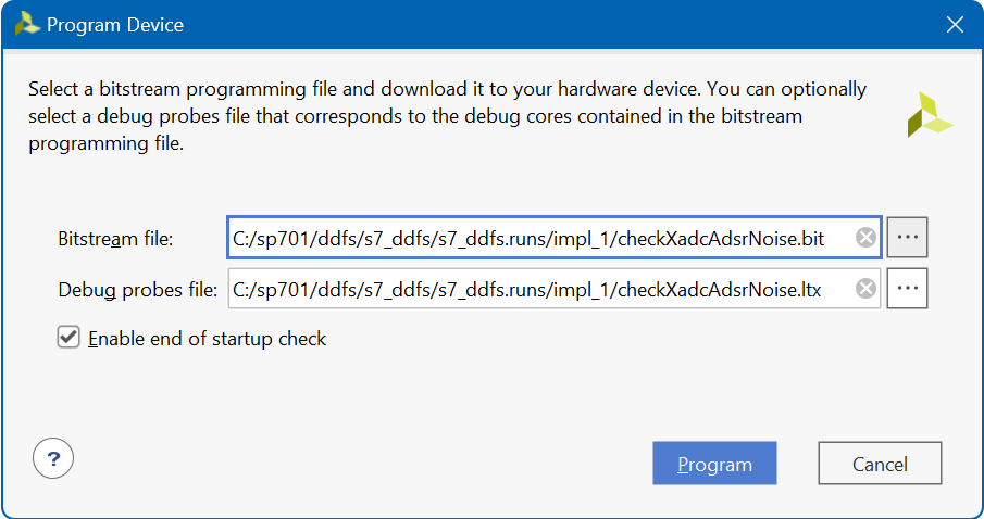
Programming device attaching debug probes file
Conclusions
This project is a new objective fulfilled for the final goal of learning SystemVerilog HDL by creating my own synthesizer designed with FPGA. Thanks to dougw and genebren for posting their blogs on the subject that I am learning and being inspired by.


