


Introduction
In the previous blog, FPGA ADSR envelope generator for sound synthesis , we discussed ADSR envelope generators. The data input to the ADSR module was hardcoded. It would be nice to be able to enter the step increments with knobs for each of the phases, attack step, decay step, sustain level and release step.
The Spartan-7 FPGA belonging to the AMD Xilinx FPGA 7 series has an integrated analog-to-digital converter (XADC) that we are going to use to read the values of various voltage dividers controlled by potentiometers.
An Analog to Digital Converter (ADC) is a circuit that digitizes a continuous analog signal by converting its voltage level to a discrete digital quantity.
In this blog we will learn how to configure the XADC IP module using the wizard integrated in the Vivado development tool. The XADC module is highly configurable and this wizard will allow us to automate the creation of an XADC module configuration wrapper.
In the image testing the XADC channels on the Digilent Arty S7 50 board with several 10K lineal rotary potmeters.

Table of Contents
- Introduction
- Intro to the ADMD Xilinx 7 series FPGA XADC
- XADC IP Wizard
- Step by Step XADC IP core configuration
- XADC Port Descriptions
- Files created with .xic and HDL extension
- Connecting the potentiometers with the Arsty S7 50 board
- Digilent Arty S7 50 Shield Analog I/O
- Constraints file
- Demo circuit
- SystemVerilog Study Notes Chapters
Intro to the ADMD Xilinx 7 series FPGA XADC
AMD Xilinx 7 series FPGA devices contain a macro cell, XADC; which provides basic analog-to-digital conversion functionality. It is a dual 12-bit, 1 MSPS analog-to-digital converter with on-chip sensors.
The diagram of an ADMD Xilinx 7 series FPGA XADC macro is shown in the figure

(1) Zynq-7000 SoC devices only.
source: XADC Overview • 7 Series FPGAs (xilinx.com)
It consists of five major parts:
- Dual ADCs
- On-chip sensors and alarm
- Analog multiplexers
- Control register and status register
- DRP (dynamic reconfiguration port) interface.
The two ADCs are the main components. The ADC has a resolution of 12 bits and a sampling rate of 1 M SPS (samples per second). It utilizes a differential input structure, in which the voltage difference between two pins (the plus and minus inputs) is used for measurement. The maximum swing of the inputs is 1.0 V. The input can be configured as unipolar mode, in which the voltage range is between 0.0 and +1.0 V, or as bipolar mode, with a voltage range between -0.5 V and 0.5 V
An analog multiplexer selects a specific input signal and converts it to the output. The multiplexer allows multiple analog input channels to be routed to a single ADC. The sequencer mode allows to share a fast ADC with multiple low-data rate channels. The XADC can allocate one dedicated analog channel, 16 auxiliary analog channels and internal temperature and voltage sensor readings.
In sequencer mode we can select the needed channels and sensors. The I/O pins for the unused auxiliary analog channels can be configures as regular digital I/O pins.
XADC IP Wizard
Xilinx provides a collection of Intellectual Property (IP) cores. Certain FPGA's macro cells, such as the FPGA Series 7 XADC, can only be incorporated as a Xilinx IP core.
We have several ways to instantiate a Xilinx IP core:
- Copy and modify a predefined HDL template.
- Instantiate a single IP instance with the IP Catalog.
- Use the IP Integrator utility.
Vivado provides the IP catalog utility which has various wizard programs to configure an IP core and generate an HDL file. In order to instantiate an XADC IP core we must follow these steps:
- Invoke the XADC wizard to configure that IP core.
- Generate the HDL file.
- Instantiate the IP as a component of the top-level HDL file.
The wizard creates a file with extension of .xic. This one is then used as a blueprint to generate HDL files
More info: xadc-wizard.html
Step by Step XADC IP core configuration
From Vivado In the Flow Navigator subwindow expand PROJECT MANAGER and select IP Catalog.
Select the FPGA Features and Design, then XADC, then XADC wizard

An XADC Wizard dialog appears:
- Enter the Component Name: xadc_adsr
- Select DRP as interface.
- Select Continuous Mode in Timing Mode.
- Select Channel Sequencer in Startup Channel Selection

In the ADC Setup confirm that Sequencer Mode is Continuous.

We don't need any alarms. Deselect all the Alarms in the Alarms section.

In the Channel Sequencer page, uncheck Bipolar option in all the channels.
Check the following boxes in Channel Enable: VP, VN, vauxp0/vauxn0, vauxp1/vauxn1, vauxp2/vauxn2, vauxp3/vauxn3, vauxp8/vauxn8, vauxp9/vauxn9, vauxp2/vauxn2, vauxp3/vauxn3.
This selection is for the Digilent ARTY S7 50.
The Digilent Arty S7 50 has 6 Single-ended 0-3.3V Analog inputs to XADC and 3 Differential 0-1.0V Analog input pairs to XADC
- A0-A5 Single-Ended Analog Input. On the pins labeled A0-A5 Digilent use an external circuit to scale down the input voltage from 3.3V.
- A6-A9 Differential Analog Input: The pins labeled A6-A9 are connected directly to 2 pairs of analog capable pins on the FPGA via an anti-aliasing filter. These pairs of pins can be used as differential analog inputs with a voltage difference between 0-1V. The even numbers are connected to the positive pins of the pair and the odd numbers are connected to the negative pins (so A6 and A7 form an analog input pair with A6 being positive and A7 being negative).
- V_P, V_N Dedicated Differential Analog Input. The pins labeled V_P and V_N are connected to the VP_0 and VN_0 dedicated analog inputs of the FPGA. This pair of pins can also be used as a differential analog input with voltage between 0-1V, but they cannot be used as Digital I/O.

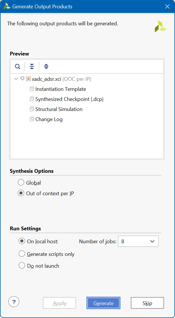
Check the OK button. And then the Generate button to generate the xadc_adsr.xci file and HDL files.
XADC Port Descriptions
For reference and better understanding of the HDL files created by the wizard, this table contains the description of all XADC module ports.
Files created with .xic and HDL extension
Within the Sources panel under Design Sources we can find the new files.

This is the Verilog HDL file created by the wizard:
// file: xadc_adsr.v
// (c) Copyright 2009 - 2013 Xilinx, Inc. All rights reserved.
//
// This file contains confidential and proprietary information
// of Xilinx, Inc. and is protected under U.S. and
// international copyright and other intellectual property
// laws.
//
// DISCLAIMER
// This disclaimer is not a license and does not grant any
// rights to the materials distributed herewith. Except as
// otherwise provided in a valid license issued to you by
// Xilinx, and to the maximum extent permitted by applicable
// law: (1) THESE MATERIALS ARE MADE AVAILABLE "AS IS" AND
// WITH ALL FAULTS, AND XILINX HEREBY DISCLAIMS ALL WARRANTIES
// AND CONDITIONS, EXPRESS, IMPLIED, OR STATUTORY, INCLUDING
// BUT NOT LIMITED TO WARRANTIES OF MERCHANTABILITY, NON-
// INFRINGEMENT, OR FITNESS FOR ANY PARTICULAR PURPOSE; and
// (2) Xilinx shall not be liable (whether in contract or tort,
// including negligence, or under any other theory of
// liability) for any loss or damage of any kind or nature
// related to, arising under or in connection with these
// materials, including for any direct, or any indirect,
// special, incidental, or consequential loss or damage
// (including loss of data, profits, goodwill, or any type of
// loss or damage suffered as a result of any action brought
// by a third party) even if such damage or loss was
// reasonably foreseeable or Xilinx had been advised of the
// possibility of the same.
//
// CRITICAL APPLICATIONS
// Xilinx products are not designed or intended to be fail-
// safe, or for use in any application requiring fail-safe
// performance, such as life-support or safety devices or
// systems, Class III medical devices, nuclear facilities,
// applications related to the deployment of airbags, or any
// other applications that could lead to death, personal
// injury, or severe property or environmental damage
// (individually and collectively, "Critical
// Applications"). Customer assumes the sole risk and
// liability of any use of Xilinx products in Critical
// Applications, subject only to applicable laws and
// regulations governing limitations on product liability.
//
// THIS COPYRIGHT NOTICE AND DISCLAIMER MUST BE RETAINED AS
// PART OF THIS FILE AT ALL TIMES.
`timescale 1ns / 1 ps

(* CORE_GENERATION_INFO = "xadc_adsr,xadc_wiz_v3_3_8,{component_name=xadc_adsr,enable_axi=false,enable_axi4stream=false,dclk_frequency=100,enable_busy=true,enable_convst=false,enable_convstclk=false,enable_dclk=true,enable_drp=true,enable_eoc=true,enable_eos=true,enable_vbram_alaram=false,enable_vccddro_alaram=false,enable_Vccint_Alaram=false,enable_Vccaux_alaram=false,enable_vccpaux_alaram=false,enable_vccpint_alaram=false,ot_alaram=false,user_temp_alaram=false,timing_mode=continuous,channel_averaging=None,sequencer_mode=on,startup_channel_selection=contineous_sequence}" *)


module xadc_adsr
          (
          daddr_in,            // Address bus for the dynamic reconfiguration port
          dclk_in,             // Clock input for the dynamic reconfiguration port
          den_in,              // Enable Signal for the dynamic reconfiguration port
          di_in,               // Input data bus for the dynamic reconfiguration port
          dwe_in,              // Write Enable for the dynamic reconfiguration port
          reset_in,            // Reset signal for the System Monitor control logic
          vauxp0,              // Auxiliary channel 0
          vauxn0,
          vauxp1,              // Auxiliary channel 1
          vauxn1,
          vauxp2,              // Auxiliary channel 2
          vauxn2,
          vauxp3,              // Auxiliary channel 3
          vauxn3,
          vauxp8,              // Auxiliary channel 8
          vauxn8,
          vauxp9,              // Auxiliary channel 9
          vauxn9,
          vauxp10,             // Auxiliary channel 10
          vauxn10,
          vauxp11,             // Auxiliary channel 11
          vauxn11,
          busy_out,            // ADC Busy signal
          channel_out,         // Channel Selection Outputs
          do_out,              // Output data bus for dynamic reconfiguration port
          drdy_out,            // Data ready signal for the dynamic reconfiguration port
          eoc_out,             // End of Conversion Signal
          eos_out,             // End of Sequence Signal
          alarm_out,           // OR'ed output of all the Alarms
          vp_in,               // Dedicated Analog Input Pair
          vn_in);

          input [6:0] daddr_in;
          input dclk_in;
          input den_in;
          input [15:0] di_in;
          input dwe_in;
          input reset_in;
          input vauxp0;
          input vauxn0;
          input vauxp1;
          input vauxn1;
          input vauxp2;
          input vauxn2;
          input vauxp3;
          input vauxn3;
          input vauxp8;
          input vauxn8;
          input vauxp9;
          input vauxn9;
          input vauxp10;
          input vauxn10;
          input vauxp11;
          input vauxn11;
          input vp_in;
          input vn_in;

          output busy_out;
          output [4:0] channel_out;
          output [15:0] do_out;
          output drdy_out;
          output eoc_out;
          output eos_out;
          output alarm_out;

        wire FLOAT_VCCAUX;
        wire FLOAT_VCCINT;
        wire FLOAT_TEMP;
          wire GND_BIT;
    wire [2:0] GND_BUS3;
          assign GND_BIT = 0;
    assign GND_BUS3 = 3'b000;
          wire [15:0] aux_channel_p;
          wire [15:0] aux_channel_n;
          wire [7:0]  alm_int;
          assign alarm_out = alm_int[7];
          assign aux_channel_p[0] = vauxp0;
          assign aux_channel_n[0] = vauxn0;

          assign aux_channel_p[1] = vauxp1;
          assign aux_channel_n[1] = vauxn1;

          assign aux_channel_p[2] = vauxp2;
          assign aux_channel_n[2] = vauxn2;

          assign aux_channel_p[3] = vauxp3;
          assign aux_channel_n[3] = vauxn3;

          assign aux_channel_p[4] = 1'b0;
          assign aux_channel_n[4] = 1'b0;

          assign aux_channel_p[5] = 1'b0;
          assign aux_channel_n[5] = 1'b0;

          assign aux_channel_p[6] = 1'b0;
          assign aux_channel_n[6] = 1'b0;

          assign aux_channel_p[7] = 1'b0;
          assign aux_channel_n[7] = 1'b0;

          assign aux_channel_p[8] = vauxp8;
          assign aux_channel_n[8] = vauxn8;

          assign aux_channel_p[9] = vauxp9;
          assign aux_channel_n[9] = vauxn9;

          assign aux_channel_p[10] = vauxp10;
          assign aux_channel_n[10] = vauxn10;

          assign aux_channel_p[11] = vauxp11;
          assign aux_channel_n[11] = vauxn11;

          assign aux_channel_p[12] = 1'b0;
          assign aux_channel_n[12] = 1'b0;

          assign aux_channel_p[13] = 1'b0;
          assign aux_channel_n[13] = 1'b0;

          assign aux_channel_p[14] = 1'b0;
          assign aux_channel_n[14] = 1'b0;

          assign aux_channel_p[15] = 1'b0;
          assign aux_channel_n[15] = 1'b0;
XADC #(
        .INIT_40(16'h0000), // config reg 0
        .INIT_41(16'h21AF), // config reg 1
        .INIT_42(16'h0400), // config reg 2
        .INIT_48(16'h0800), // Sequencer channel selection
        .INIT_49(16'h0F0F), // Sequencer channel selection
        .INIT_4A(16'h0000), // Sequencer Average selection
        .INIT_4B(16'h0000), // Sequencer Average selection
        .INIT_4C(16'h0000), // Sequencer Bipolar selection
        .INIT_4D(16'h0000), // Sequencer Bipolar selection
        .INIT_4E(16'h0000), // Sequencer Acq time selection
        .INIT_4F(16'h0000), // Sequencer Acq time selection
        .INIT_50(16'hB5ED), // Temp alarm trigger
        .INIT_51(16'h57E4), // Vccint upper alarm limit
        .INIT_52(16'hA147), // Vccaux upper alarm limit
        .INIT_53(16'hCA33),  // Temp alarm OT upper
        .INIT_54(16'hA93A), // Temp alarm reset
        .INIT_55(16'h52C6), // Vccint lower alarm limit
        .INIT_56(16'h9555), // Vccaux lower alarm limit
        .INIT_57(16'hAE4E),  // Temp alarm OT reset
        .INIT_58(16'h5999), // VCCBRAM upper alarm limit
        .INIT_5C(16'h5111),  //  VCCBRAM lower alarm limit
        .SIM_DEVICE("7SERIES"),
        .SIM_MONITOR_FILE("design.txt")
)

inst (
        .CONVST(GND_BIT),
        .CONVSTCLK(GND_BIT),
        .DADDR(daddr_in[6:0]),
        .DCLK(dclk_in),
        .DEN(den_in),
        .DI(di_in[15:0]),
        .DWE(dwe_in),
        .RESET(reset_in),
        .VAUXN(aux_channel_n[15:0]),
        .VAUXP(aux_channel_p[15:0]),
        .ALM(alm_int),
        .BUSY(busy_out),
        .CHANNEL(channel_out[4:0]),
        .DO(do_out[15:0]),
        .DRDY(drdy_out),
        .EOC(eoc_out),
        .EOS(eos_out),
        .JTAGBUSY(),
        .JTAGLOCKED(),
        .JTAGMODIFIED(),
        .OT(),
        .MUXADDR(),
        .VP(vp_in),
        .VN(vn_in)
          );

endmodule
Connecting the potentiometers with the Arsty S7 50 board
The Digilent Arty S7 50 has 6 Single-ended 0-3.3V Analog inputs to XADC and 3 Differential 0-1.0V Analog input pairs to XADC.
- A0-A5 Single-Ended Analog
- A6-A9 Differential Analog Input
- V_P, V_N Dedicated Differential Analog Input
- XGND XADC Analog Ground Connected to net used to drive the XADC ground reference on the FPGA (VREFN)
- XVREF XADC Analog Voltage Reference Connected to 1.25 V, 25mA rail used to drive the XADC voltage reference on the FPGA (VREFP)

| Pin Name | Shield Function | Shared Connections |
|---|---|---|
| A0-A5 | Single-Ended Analog Input | – |
| IO0-IO9, A (IO42), A10-A11 | General purpose I/O pins | – |
| IO26-IO33 | General purpose I/O pins | Pmod JD |
| IO34-IO41 | General purpose I/O pins | Pmod JC |
| SCL | I2C Clock | – |
| SDA | I2C Data | – |
| IO13 | General purpose I/O, SPI Clock | SCLK pin of SPI Connector |
| IO11 | General purpose I/O, SPI Data out | MOSI pin of SPI Connector |
| IO12 | General purpose I/O, SPI Data in | MISO pin of SPI Connector |
| IO10 | General purpose I/O, SPI Slave Select | SS pin of SPI Connector |
| A6-A9 | Differential Analog Input | – |
| V_P, V_N | Dedicated Differential Analog Input | – |
| XGND | XADC Analog Ground | – |
| XVREF | XADC Analog Voltage Reference | – |
| N/C | Not Connected | – |
| IOREF | Digital I/O Voltage reference | – |
| RST | Reset to Shield | – |
| 3V3 | 3.3V Power Rail | – |
| 5V0 | 5.0V Power Rail | – |
| GND, G | Ground | – |
| VIN | Power Input | – |
Digilent Arty S7 50 Shield Analog I/O
The pins labeled A0-A9 and V_P/V_N are used as analog inputs to the XADC module of the FPGA. The FPGA expects that the inputs range from 0-1 V.
On the pins labeled A0-A5 Digilent use an external circuit to scale down the input voltage from 3.3V.
This circuit allows the XADC module to accurately measure any voltage between 0V and 3.3V (relative to the Arty S7's GND) that is applied to any of these pins. If you wish to use the pins labeled A0-A5 as Digital inputs or outputs, they are also connected directly to the FPGA before the resistor divider circuit.

The pins labeled A6-A9 are connected directly to 2 pairs of analog capable pins on the FPGA via an anti-aliasing filter. This circuit is shown in the next figure. These pairs of pins can be used as differential analog inputs with a voltage difference between 0-1V. The even numbers are connected to the positive pins of the pair and the odd numbers are connected to the negative pins (so A6 and A7 form an analog input pair with A6 being positive and A7 being negative). Note that though the pads for the capacitor are present, they are not loaded for these pins. Since the analog capable pins of the FPGA can also be used like normal digital FPGA pins, it is also possible to use these pins for Digital I/O.
The pins labeled V_P and V_N are connected to the VP_0 and VN_0 dedicated analog inputs of the FPGA. This pair of pins can also be used as a differential analog input with voltage between 0-1V, but they cannot be used as Digital I/O. The capacitor in the circuit shown in the figure for this pair of pins is loaded on the Arty S7.

Constraints file
## This file is a general .xdc for the Arty S7-50 Rev. B

## Clock Signals
set_property -dict {PACKAGE_PIN R2 IOSTANDARD SSTL135} [get_ports clk]
create_clock -period 10.000 -name sys_clk_pin -waveform {0.000 5.000} -add [get_ports clk]

## Switches
set_property -dict {PACKAGE_PIN H14 IOSTANDARD LVCMOS33} [get_ports {sw[0]}]
set_property -dict {PACKAGE_PIN H18 IOSTANDARD LVCMOS33} [get_ports {sw[1]}]
set_property -dict {PACKAGE_PIN G18 IOSTANDARD LVCMOS33} [get_ports {sw[2]}]
set_property -dict {PACKAGE_PIN M5 IOSTANDARD SSTL135} [get_ports {sw[3]}]

## LEDs
set_property -dict {PACKAGE_PIN E18 IOSTANDARD LVCMOS33} [get_ports {led[0]}]
set_property -dict {PACKAGE_PIN F13 IOSTANDARD LVCMOS33} [get_ports {led[1]}]
set_property -dict {PACKAGE_PIN E13 IOSTANDARD LVCMOS33} [get_ports {led[2]}]
set_property -dict {PACKAGE_PIN H15 IOSTANDARD LVCMOS33} [get_ports {led[3]}]

## RGB LEDs
#set_property -dict { PACKAGE_PIN J15   IOSTANDARD LVCMOS33 } [get_ports { led0_r }]; #IO_L23N_T3_FWE_B_15 Sch=led0_r
set_property -dict { PACKAGE_PIN G17   IOSTANDARD LVCMOS33 } [get_ports { led[4] }]; #IO_L14N_T2_SRCC_15 Sch=led0_g
#set_property -dict { PACKAGE_PIN F15   IOSTANDARD LVCMOS33 } [get_ports { led0_b }]; #IO_L13N_T2_MRCC_15 Sch=led0_b
#set_property -dict { PACKAGE_PIN E15   IOSTANDARD LVCMOS33 } [get_ports { led1_r }]; #IO_L15N_T2_DQS_ADV_B_15 Sch=led1_r
set_property -dict { PACKAGE_PIN F18   IOSTANDARD LVCMOS33 } [get_ports { led[5] }]; #IO_L16P_T2_A28_15 Sch=led1_g
#set_property -dict { PACKAGE_PIN E14   IOSTANDARD LVCMOS33 } [get_ports { led1_b }]; #IO_L15P_T2_DQS_15 Sch=led1_b


## Buttons
set_property -dict {PACKAGE_PIN G15 IOSTANDARD LVCMOS33} [get_ports {btn[0]}]
set_property -dict {PACKAGE_PIN K16 IOSTANDARD LVCMOS33} [get_ports {btn[1]}]
set_property -dict {PACKAGE_PIN J16 IOSTANDARD LVCMOS33} [get_ports {btn[2]}]
set_property -dict {PACKAGE_PIN H13 IOSTANDARD LVCMOS33} [get_ports {btn[3]}]


## Pmod Header JD
set_property -dict {PACKAGE_PIN V15 IOSTANDARD LVCMOS33} [get_ports audio_out]
set_property DRIVE 16 [get_ports audio_out]
set_property -dict {PACKAGE_PIN U12 IOSTANDARD LVCMOS33} [get_ports gain]
set_property -dict {PACKAGE_PIN V13 IOSTANDARD LVCMOS33} [get_ports pulse_out]
set_property -dict {PACKAGE_PIN T12 IOSTANDARD LVCMOS33} [get_ports neg_shutdown]
#set_property -dict { PACKAGE_PIN T13   IOSTANDARD LVCMOS33 } [get_ports { jd[4] }]; #IO_L22N_T3_A04_D20_14 Sch=jd7/ck_io[29]
#set_property -dict { PACKAGE_PIN R11   IOSTANDARD LVCMOS33 } [get_ports { jd[5] }]; #IO_L23P_T3_A03_D19_14 Sch=jd8/ck_io[28]
#set_property -dict { PACKAGE_PIN T11   IOSTANDARD LVCMOS33 } [get_ports { jd[6] }]; #IO_L23N_T3_A02_D18_14 Sch=jd9/ck_io[27]
#set_property -dict { PACKAGE_PIN U11   IOSTANDARD LVCMOS33 } [get_ports { jd[7] }]; #IO_L24P_T3_A01_D17_14 Sch=jd10/ck_io[26]


## ChipKit Single Ended Analog Inputs
## NOTE: The ck_an_p pins can be used as single ended analog inputs with voltages from 0-3.3V (Chipkit Analog pins A0-A5).
## These signals should only be connected to the XADC core. When using these pins as digital I/O, use pins ck_io[14-19].
set_property -dict { PACKAGE_PIN B13   IOSTANDARD LVCMOS33 } [get_ports { vauxp0 }]; #IO_L1P_T0_AD0P_15 Sch=ck_an_p[0]
set_property -dict { PACKAGE_PIN A13   IOSTANDARD LVCMOS33 } [get_ports { vauxn0 }]; #IO_L1N_T0_AD0N_15 Sch=ck_an_n[0]
set_property -dict { PACKAGE_PIN B15   IOSTANDARD LVCMOS33 } [get_ports { vauxp1 }]; #IO_L3P_T0_DQS_AD1P_15 Sch=ck_an_p[1]
set_property -dict { PACKAGE_PIN A15   IOSTANDARD LVCMOS33 } [get_ports { vauxn1 }]; #IO_L3N_T0_DQS_AD1N_15 Sch=ck_an_n[1]
set_property -dict { PACKAGE_PIN E12   IOSTANDARD LVCMOS33 } [get_ports { vauxp9 }]; #IO_L5P_T0_AD9P_15 Sch=ck_an_p[2]
set_property -dict { PACKAGE_PIN D12   IOSTANDARD LVCMOS33 } [get_ports { vauxn9 }]; #IO_L5N_T0_AD9N_15 Sch=ck_an_n[2]
set_property -dict { PACKAGE_PIN B17   IOSTANDARD LVCMOS33 } [get_ports { vauxp2 }]; #IO_L7P_T1_AD2P_15 Sch=ck_an_p[3]
set_property -dict { PACKAGE_PIN A17   IOSTANDARD LVCMOS33 } [get_ports { vauxn2 }]; #IO_L7N_T1_AD2N_15 Sch=ck_an_n[3]
set_property -dict { PACKAGE_PIN C17   IOSTANDARD LVCMOS33 } [get_ports { vauxp10 }]; #IO_L8P_T1_AD10P_15 Sch=ck_an_p[4]
set_property -dict { PACKAGE_PIN B18   IOSTANDARD LVCMOS33 } [get_ports { vauxn10 }]; #IO_L8N_T1_AD10N_15 Sch=ck_an_n[4]
set_property -dict { PACKAGE_PIN E16   IOSTANDARD LVCMOS33 } [get_ports { vauxp11 }]; #IO_L10P_T1_AD11P_15 Sch=ck_an_p[5]
set_property -dict { PACKAGE_PIN E17   IOSTANDARD LVCMOS33 } [get_ports { vauxn11 }]; #IO_L10N_T1_AD11N_15 Sch=ck_an_n[5]

## Dedicated Analog Inputs
set_property -dict { PACKAGE_PIN J10   } [get_ports { vp_in }]; #IO_L1P_T0_AD4P_35 Sch=v_p
set_property -dict { PACKAGE_PIN K9    } [get_ports { vn_in }]; #IO_L1N_T0_AD4N_35 Sch=v_n

## ChipKit Digital I/O On Inner Analog Header
## NOTE: These pins will need to be connected to the XADC core when used as differential analog inputs (Chipkit analog pins A6-A11)
set_property -dict { PACKAGE_PIN B14   IOSTANDARD LVCMOS33 } [get_ports { vauxp8 }]; #IO_L2P_T0_AD8P_15 Sch=ad_p[8]
set_property -dict { PACKAGE_PIN A14   IOSTANDARD LVCMOS33 } [get_ports { vauxn8 }]; #IO_L2N_T0_AD8N_15 Sch=ad_n[8]
set_property -dict { PACKAGE_PIN D16   IOSTANDARD LVCMOS33 } [get_ports { vauxp3 }]; #IO_L9P_T1_DQS_AD3P_15 Sch=ad_p[3]
set_property -dict { PACKAGE_PIN D17   IOSTANDARD LVCMOS33 } [get_ports { vauxn3 }]; #IO_L9N_T1_DQS_AD3N_15 Sch=ad_n[3]


## Configuration options, can be used for all designs
set_property BITSTREAM.CONFIG.CONFIGRATE 50 [current_design]
set_property CONFIG_VOLTAGE 3.3 [current_design]
set_property CFGBVS VCCO [current_design]
set_property BITSTREAM.CONFIG.SPI_BUSWIDTH 4 [current_design]
set_property CONFIG_MODE SPIx4 [current_design]

## SW3 is assigned to a pin M5 in the 1.35v bank. This pin can also be used as
## the VREF for BANK 34. To ensure that SW3 does not define the reference voltage
## and to be able to use this pin as an ordinary I/O the following property must
## be set to enable an internal VREF for BANK 34. Since a 1.35v supply is being
## used the internal reference is set to half that value (i.e. 0.675v). Note that
## this property must be set even if SW3 is not used in the design.
set_property INTERNAL_VREF 0.675 [get_iobanks 34]


set_property BITSTREAM.GENERAL.COMPRESS TRUE [current_design]
Channel selection
| Ports | Package pin | Address Dec | Address hex |
| A0 |
IO_L1P_T0_AD0P_15 IO_L1P_T0_AD0N_15 |
16 | 8'h10 |
| A1 |
IO_L3P_T0_DQS_AD1P_15 IO_L3N_T0_DQS_AD1N_15 |
17 | 8'h11 |
| A2 |
IO_L5P_T0_AD9P_15 IO_L5N_T0_AD9N_15 |
25 | 8'h19 |
| A3 |
IO_L7P_T1_AD2P_15 IO_L7N_T1_AD2N_15 |
18 | 8'h12 |
| A4 |
IO_L8P_T1_AD10P_15 IO_L8N_T1_AD10N_15 |
26 | 8'h1A |
| A5 |
IO_L10P_T1_AD11P_15 IO_L10N_T1_AD11N_15 |
27 | 8'h1B |
| A6-A7 differential |
IO_L2P_T0_AD8P_15 IO_L2N_T0_AD8N_15 |
24 | 8'h18 |
| A8-A9 differential |
IO_L9P_T1_DQS_AD3P_15 IO_L9N_T1_DQS_AD3N_15 |
19 | 8'h13 |
| Dedicated V differential |
IO_L1P_T0_AD4P_35 IO_L1N_T0_AD4N_35 |
03 | 8'h03 |
Demo circuit
A top level design for reading values off of the XADC. The 6 User LEDs increment from top right to left then bottom right to left as the voltage difference on the selected XADC pins gets larger.
Selecting a channel: To display a different channel on the LEDs, change the user switches to the desired channel.
| Channel Pin/s | SW3 | SW2 | SW1 | SW0 |
|---|---|---|---|---|
| A0 | Up | Down | Down | Down |
| A1 | Down | Up | Down | Down |
| A2 | Down | Down | Up | Down |
| A3 | Down | Down | Down | Up |
SystemVerilog Implementation
`timescale 1ns / 1ps

module adrs_controller(
   input logic clk,
   input logic vp_in,
   input logic vn_in,
   input logic vauxp0,
   input logic vauxn0,
   input logic vauxp1,
   input logic vauxn1,
   input logic vauxp2,
   input logic vauxn2,
   input logic vauxp3,
   input logic vauxn3,
   input logic vauxp8,
   input logic vauxn8,
   input logic vauxp9,
   input logic vauxn9,
   input logic vauxp10,
   input logic vauxn10,
   input logic vauxp11,
   input logic vauxn11,

   input [3:0] sw,
   output reg [5:0] led

 );

   logic enable;
   logic ready;
   logic ready_d1;
   logic ready_rising;
   logic ready_falling;
   logic [15:0] data;
   logic [6:0] address_in;

   //xadc instantiation connect the eoc_out .den_in to get continuous conversion

    xadc_adsr xadc
        (
        .daddr_in(address_in),   // Address bus for the dynamic reconfiguration port
        .dclk_in(clk),           // Clock input for the dynamic reconfiguration port
        .den_in(enable),         // Enable Signal for the dynamic reconfiguration port
        .di_in(0),               // Input data bus for the dynamic reconfiguration port
        .dwe_in(0),              // Write Enable for the dynamic reconfiguration port
        .reset_in(0),            // Reset signal for the System Monitor control logic

        .vp_in(vp_in),          // input wire vp_in
        .vn_in(vn_in),          // input wire vn_in
        .vauxp0(vauxp0),        // input wire vauxp0
        .vauxn0(vauxn0),        // input wire vauxn0
        .vauxp1(vauxp1),        // input wire vauxp1
        .vauxn1(vauxn1),        // input wire vauxn1
        .vauxp2(vauxp2),        // input wire vauxp2
        .vauxn2(vauxn2),        // input wire vauxn2
        .vauxp3(vauxp3),        // input wire vauxp3
        .vauxn3(vauxn3),        // input wire vauxn3

        .vauxp8(vauxp8),        // input wire vauxp8
        .vauxn8(vauxn8),        // input wire vauxn8
        .vauxp9(vauxp9),        // input wire vauxp9
        .vauxn9(vauxn9),        // input wire vauxn9
        .vauxp10(vauxp10),      // input wire vauxp10
        .vauxn10(vauxn10),      // input wire vauxn10
        .vauxp11(vauxp11),      // input wire vauxp11
        .vauxn11(vauxn11),      // input wire vauxn11

        .busy_out(),            // ADC Busy signal
        .channel_out(),         // Channel Selection Outputs
        .do_out(data),          // Output data bus for dynamic reconfiguration port
        .drdy_out(ready),       // Data ready signal for the dynamic reconfiguration port

        .eoc_out(enable),       // End of Conversion Signal
        .eos_out(),             // End of Sequence Signal
        .alarm_out()            // OR'ed output of all the Alarms

    );

      always_ff @(posedge clk)
      begin
          ready_d1 <= ready;
      end

      assign ready_rising = ready && !ready_d1 ? 1'b1 : 1'b0;
      assign ready_falling = !ready && ready_d1 ? 1'b1 : 1'b0;

      //led visual dmm
      always_ff @(posedge clk)
      begin
          if (ready_rising == 1)
          begin
              case (data[15:13])
                2:  led <= 6'b000001;
                3:  led <= 6'b000011;
                4:  led <= 6'b000111;
                5:  led <= 6'b001111;
                6:  led <= 6'b011111;
                7:  led <= 6'b111111;
                default: led <= 6'b0;
              endcase
          end
          else
              led <= led;
       end

      //switch driver to choose channel
      always_ff @(posedge clk)
      begin
          if (ready_rising == 1)
          begin
            case(sw)
                8: address_in <= 8'h10; //A0
                4: address_in <= 8'h11; //A1
                2: address_in <= 8'h19; //A2
                1: address_in <= 8'h12; //A3
                default: address_in <= 8'h10; //A0
            endcase
          end
          else
            address_in <= address_in;
      end
endmodule
Demo video
SystemVerilog Study Notes Chapters
- Gate-Level Combinational Circuit
- RTL Combinational Circuit Operators
- RTL Combinational Circuit - Concurrent and Control Constructs
- Hex-Digit to Seven-Segment LED Decoder RTL Combinational Circuit
- Barrel Shifter RTL Combinational Circuit
- Simplified Floating Point Arithmetic. RTL Combinational Circuit
- BCD Number Format. RTL Combinational Circuit
- DDFS. Direct Digital Frequency Synthesis for Sound
- FPGA ADSR envelope generator for sound synthesis
- AMD Xilinx 7 series FPGAs XADC
- Building FPGA-Based Music Instrument Synthesis: A Simple Test Bench Solution
