


Semiconductors I: GaNFETs for Power Conversion
Sponsored by

As the world moves towards low emission vehicles, renewable energy, and increased industrial automation, there are new demands for improved, efficient power modules to convert electric energy to drive dynamic loads. Switching power modules are tasked to provide more efficient power conversion in challenging settings. This is driving new technologies to improve the efficiency and reliability of switch mode power supplies (SMPSs). One interesting development is the application of high-electron-mobility transistors (HEMTs) to improve the performance of solid state switches. One candidate that is entering commercial acceptance is the GaNFET (Galium-Nitride Field Effect Transistor). In this lesson, we will review the requirements of electronics in power conversion applications, the limitations of current solutions, and the potential for this new device technology. We will consider a design problem to address the selection and implementation of a power conversion module utilizing GaNFETs.
2. Objectives
Upon completion of this module, you will be able to:
 Discuss requirements for power switching
Understand the limitations of existing Silicon (Si) MOSFET technology
Describe the advantages of GaN MOSFET switches
Design a traction motor power converter for a battery electric vehicle
A GaNFET is a high-electron-mobility field effect transistor. It is designed to operate as a highly efficient and robust switch for power converters. The bulk material is much more conductive than silicon, and thus it does not dissipate much heat in the on-state. They also have a high breakdown voltage, so these devices are suitable for grid connected power conversion, or high horsepower motor drives. This makes them well suited to renewable energy and electric vehicle applications.
As the world moves towards zero emission vehicles, renewable energy, and increased industrial automation, there are new demands for improved efficient power modules to convert electric energy to dynamic loads. Switching power modules are tasked to provide more efficient power conversion in more challenging settings. Electric vehicles have severe requirements for performance and reliable operation in extreme environments. Industrial systems are becoming more automated and adaptable, requiring nimble power delivery for large scale automation and robotics. Power grids are increasingly fed by asynchronous sources like solar and wind, requiring large scale power conversion to deliver and store energy to where it is needed, when it is needed.
These applications create the need and expectation for electric power conversion systems, but the switching devices that operate at the beating heart of switch mode power supplies have reached some degree of maturity. In order to improve performance and efficiency, new technologies are being developed to stretch the operational envelope of power conversion systems.
Industrial automation requires motors and robotic actuators that can quickly change speed and deliver high mechanical torque on demand for precision positioning, processing, and agile manufacturing. Industrial motors may be large-scale DC motors, high power variable speed induction motors, or controlled torque synchronous motors. Industrial DC motors require AC-to-DC power converters. Variable speed induction motors require variable frequency AC-to-AC converters. Synchronous motors require both variable frequency AC-to-AC conversion for the field stator, and AC-to-DC conversion for the armature windings.
Electric vehicles store their power in high density and high power batteries, and drive their wheels with high torque traction motors. On board chargers require AC-to-DC conversion. Synchronous motors require high power DC-to-AC conversion. Regenerative braking requires high power AC-to-DC conversion. So battery electric vehicles (BEVs) require all manner of power conversion topologies.

Figure 1: Power flow and conversion modules for a Battery Electric Vehicle (BEV)
All these applications can benefit from high efficiency power conversion systems. Faster switching speeds allow for lighter and smaller passive filter components in the power modules. Higher conductivity (lowered output impedance) allows for less loss and more efficient power conversion, which allows for cooler operation and less stress on the switching components. Less heat loss also eliminates the need for bulky heat dissipation radiators. More robust (higher voltage) switching devices also allow for more reliable operation in severe environments, to which all these application domains are exposed.
Clearly there is a need for better solutions for high power electric conversion systems, and also there are opportunities for new technologies.
- 4.1 Comparison of Electronic Switching Devices for Switch Mode Power Systems
While switch mode power supplies add complications to power systems, their advantages are worth the added engineering. While an analysis of a SMPS is more involved, these systems have been in the field for a generation, so their operation is well understood. From the perspective of a design engineer, the choice of power switching devices comes down to optimizing the attributes of efficiency, robustness, light footprint, and scalability. To optimize efficiency, the device should have high conductivity to minimize losses and wasted heating. To optimize footprint, the device should have high speed switching to allow for smaller and lighter passive filter components. To optimize robustness, the switches should sustain high voltages in the off state and high currents in the on state. To optimize scalability, the devices should use standard fabrication techniques to leverage well developed manufacturing practices and accepted standards to validate quality and reliability.
We will consider three device families for electronic switches: IGBTs, Super-junction Si MOSFETs, and GaNFETs. The first two are well known to high power SMPS designers, while the latter is a new technology that offers unique advantages in power modules. We will address the attributes of these devices in switch mode power supply applications: efficiency measured in terms of on-state conduction; robustness measured in off state blocking voltage; and speed switching conduction states.
IGBTs
IGBTs are insulated gate bipolar transistors. They are silicon thyristors that are switched by an insulated gate like a MOSFET, but can be turned off with gate potential, unlike a thyristor. They have the advantages of very high blocking voltage and high conduction in the on state. Their disadvantage is that they have limited switching speeds, due to gate response.
Super-junction Si MOSFETs
Super-junction Si MOSFETs are an excellent choice, but they have issues of limited conductivity depending on the properties of the depletion layer channel. Also, MOSFETs have limited blocking voltage due to their doped charge carriers.
GaN FETs
GaNFETs employ a high-electron-mobility transistor that allows for excellent conductivity in the on-state, and high voltage blocking in the off-state, so they offer high efficiency and robustness. GaN is an exotic semiconductor, but the crystal is grown on a silicon substrate, so processing uses industry standard 200 mm fabrication techniques. While the GaN HEMT offers superior conductivity and high blocking voltage, they are usually coupled with a low voltage silicon MOSFET in cascade to leverage the high switching speeds and isolated gate of silicon MOSFETs. Compared to Si FETs in a simple buck converter, GaNFET losses are significantly lower due to the absence of reverse recovery losses and switching crossover losses. Amongst the various technologies, gallium nitride (GaN) technology shows the greatest performance benefits when compared to silicon (Si) and silicon carbide (SiC) solutions. Specifically, GaN field-effect transistors (FETs) deliver the best efficiency with low system costs, while making systems lighter, smaller, and cooler.
| Conduction | Blocking | Speed | Scalability | |
|---|---|---|---|---|
| IGBT | Fair | Good | Good | Good |
| Super-junction Si MOSFET | Good | Fair | Excellent | Excellent |
| GaNFET | Excellent | Excellent | Excellent | Fair |
Table 1: Comparision of Switching Devices
- 4.2 Semiconductor Materials for HEMT Devices
There are many candidate materials for HEMT devices. Silicon is a natural semiconductor because it has an atomic arrangement with the valence bands completely filled with electrons. Germanium shares the same property in group 14 of the periodic table, so it is sometimes used as a semiconductor. In order to improve the conductivity of silicon, the pure crystal is "doped" with atoms from the 15th group in the periodic table (Nitrogen, Phosphorus, and Arsenic) to add donor electrons to the material. These are called "n donors." Alternatively, the Silicon semiconductor can be "doped" with materials from the 13th group (Boron, Aluminum, or Gallium), which lack a single valence electron and thus form electron "holes" and are called "p donors." The lack of a valence electron in the crystal lattice effectively makes for a positive charge in the bulk semiconductor.
Semiconductors can also be formed by an even mix of group 13 and 15 elements to form an electrically neutral semiconductor. GaN (Gallium-Nitride) is a good candidate material because the gallium is electrically stable, while the nitrogen has a high ionization energy. This gives the material a high electron mobility with a large energy gap. This translates into better conduction and higher voltage ratings.
- 4.3 Commercial GaN Devices
The demand for high power, high performance switching devices has led to the development of commercially available GaNFET devices. Nexperia has developed a family of GaNFET devices tailored to the high power SMPS applications. These are listed in Table 2.
| Part Number | Vbr (V) | Rdson (mOhm) | Package |
|---|---|---|---|
| GAN063-650WSA | 650 | 50 | TO-247 |
| GAN041-650WSB | 650 | 35 | TO-247 |
| GAN039-650NBB | 650 | 33 | CCPAK1212 |
| GAN039-650NTB | 650 | 33 | CCPAK1212i |
| GAN039-650NBBA | 650 | 33 | CCPAK1212 |
| GAN039-650NTBA | 650 | 33 | CCPAK1212i |
Table 2: Nexperia GaNFET Devices
They are all rated to 650 VDC off-state blocking voltage. This is suitable for sustaining 230 VAC line voltages where the peak-to-peak voltages are 650 V. (The equation for converting VAC in RMS to peak to peak voltage is to multiple by twice the square root of two.) They are rated to sustain surge voltages up to 800 VDC in transient mode. They all have very low on-state resistance, on the order of 33 milliOhms, so they offer excellent conductivity and low losses from power dissipation. The "A" suffix is attached to automotive grade parts that are tested to the AEC-Q101 standards.
The main differences are in the packaging. The first offerings are in the industry standard T0-247 package, which is very familiar to a power electronics designer. It has a 16mm square metal tab which is electrically connected to the source terminal, which provides excellent heat transfer. The pinout differs slightly from the normal power silicon power MOSFETs in that the gate has been moved to pin 1, the source at pin 2, and the drain at pin 3. This allows a physical separation of the input and output circuits to mitigate feedback and ringing in the switching circuit.
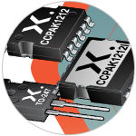
The high current and high voltage of the device pushes the limits of conventional packaging in high frequency switch mode power supplies. To address the enhanced performance, new power architectures have been designed. Nexperia has introduced a new copper-clip package to handle the high power of GaNFETs. The CCPAK is a 12mm by 12 mm surface-mounted device with the copper electrical leads clipped directly to the die, so that there are no wire-bonds. This allows for less inductance in the input circuit and less resistance to the output circuit for better stability and efficiency. This also allows for lower thermal resistance between the die and the heat sink. The "i" designation refers to an insulated configuration where the die is flipped to allow heat dissipation through the encapsulated top, rather than the electrically connected "source" pad.
Switch mode power design is a daunting task. In theory, high efficiency is achieved by maintaining the device in the loss-less off-state, or the low-loss on-state. Higher switching frequencies are desired to allow for less bulky filter components (less iron and fewer wires in the inductors and smaller capacitors). SMPSs are often operated at 100 KiloHertz, which may seem innocuous to the casual circuit designer, but the transitions need to take place at tens of MegaHertz to maintain operation in either switched state. If the circuit operates at too high a speed, then the drive circuit is subject to ringing or "bouncing." That can add many false transitions that force the device into the linear or loss-y mode. On the other hand, if the drive circuit is tuned down and overly snubbed, the state transitions are slow and the device spends more time in the loss-y linear range. Textbooks have been written on this subject, so the interested reader can find more useful information on the topic on the Nexperia and e14 websites.
In this section, we will develop a power converter for the drive motor of a battery electric vehicle. To begin, suppose we are designing a power converter to drive a new battery electric vehicle with the following specifications:
100 KW Synchronous Motor
40 KWh Lithium-Ion Battery
400 VDC battery bus
We need to create a power converter to translate the battery energy into vehicular kinetic energy. Let's answer the pertinent questions:
Q1: Can we use GaNFETs to drive the motor?
Q2: If so, how many GaN devices are required?
Q3: How much power dissipation should we allow for?
A synchronous motor has three phase AC delta connected stator windings and a DC armature winding. Addressing the problem of the stator field, we need to generate alternating current from the DC battery. Because the magnetic field needs to reverse with the alternating current, we need a full bridge driver that can deliver full current to the motor in both directions. A full bridge driver requires four switches for each phase winding.

Figure 2: Diagram of a GaNFET full bridge implementation
The GaNFET is coupled internally with an n-channel SiMOSFET. The typical implementation for the device is as a low side switch, but we can use the GaN device as a high side switch with some exotic gate drive magic. Luckily, we can specify a gate driver chip that operates the n-channel MOSFET as both a high-side switch and low-side switch in a full bridge implementation.
From the list of candidate devices in Table 2, a good choice would be the GAN039-650NTBA. This device has a low 39 milliOhm on-state resistance (Rdson), can block 650 volts in the off-state (Vdsmax), and has been tested to the automotive standard AEC-Q101. The CCPAK1212I package has an insulated thermal path through the top of the device, which allows us to use one heat transfer means for all the devices in the full bridge implementation.
A1: Yes, we can use the GaNFET to drive the motor.
The synchronous motor has three field windings in a "Wye" arrangement, so the motor power is divided equally between the three field windings as shown in Figure 2. That requires 33KW (100KW/3) of power delivered to each winding. From the power bus at 400 VDC we need 82.5 Amps (I=P/V) in each phase. Technically, because the power is delivered in pulse with modulated AC, the peak current requirement for each phase will be 116 Amps Peak (Ipeak=Irms*sqrt(2)). The maximum rating for on-state current of the device is 60 amps (Idmax), so we would need two devices for each switch in the driver bridge. With the correct precautions, the devices can be run in parallel. That makes two devices per switch in the bridge circuit, times two switches per phase, times three phase switches per full bridge amplifier, (2x2x3) which makes for twelve (12) GaNFETs in our implementation.
A2: We would need 12 GAN039-650NTBA devices to deliver three phase AC at rated power to the synchronous motor.
Now that we have established the motor drive current through the devices, we can compute the power dissipation required at peak power for the power converter.

Figure 3: Equivalent Circuit for Power Calculation (the Battery is 400 Volts, the motor winding is modeled as a 10 Ohm resistor, and the GaNFETs in the on-state are modeled as 39 Ohm resistors)
Each of the three full bridge drives will have two switches on when the current is forward, and two switches off when the current is reversed. In either direction, the field current for each phase will flow through two devices in parallel on the high side and two devices in parallel on the low side. An equivalent circuit is shown in Figure 3.
At full power, each device would carry half of the full current, about 40 amps each. Assuming the worst case on-state resistance (Rdson=39 mOhms), the power dissipation of each device would generate heating of 62 Watts per device (P=I^2 R). The device is rated for 300 Watts of power dissipation, so we are well within the operational envelope. At peak power, half of the switching in the bridge will be conducting, so that makes for six conducting devices at full power. A total of 372 Watts of waste heat needs to be dissipated.
A3: The system as designed will dissipate 372 Watts of waste heat at full power conditions.
With that, we can sit down at the drawing board and draw up a working prototype power inverter for our new battery electric vehicle drive.
Conclusion
Switch mode power supplies are seeing increased use in new markets, as the need for more efficient and reliable power conversion continues to grow, and new technologies will become more commercially viable to fill this need. We hope this Essentials has whetted your appetite to develop new applications and the potential of power conversion in your project designs. More information is available at the Nexperia and e14 websites.
HEMT: High-electron-mobility transistor
SMPS: Switch Mode Power Supply
MOSFET: Metal-Oxide-Silicon Field Effect Transistor
BEV: Battery Electric Vehicle
IGBT: Insulate-Gate Biploar Transistor
Thyristor: Silicon Controlled Rectifier
GaNFET: Gallium-Arsenide Field Effect Transistor
AEC-Q101: Automotive Electronics Council - Failure Mode Based Tests for Electronic Devices
*Trademark. is a trademark of Nexperia Inc. Other logos, product and/or company names may be trademarks of their respective owners.
Shop our wide range of diodes, Power Mosfets, Transistors, Logic ICs, Power Management ICs, and GaN FETs by Nexperia.
Test Your KnowledgeBack to Top

Are you ready to demonstrate your GaNFETs knowledge? Then take this 15-question quiz to see how much you've learned. To earn the Semiconductors I Badge, read through the learning module, attain 100% on the Quiz, leave us some feedback in the comments section, and give the learning module a star rating.
| Semiconductors I.pdf |

Top Comments