


Introduction
Surface-mounted Chip Antennas have helped incorporate wireless solutions in applications having challenges in board space and power resource limitations. In this article, we learn about the best practices for designing a chip antenna on the PCB of an RF radio.
Key parameters that Affect Antenna Performance
Antenna selection is based on the protocol and wireless standard used for communication. Important characteristics that need to be considered are Directivity, Polarization, Input Impedance, Frequency Band, Bandwidth, Radiated Power, Gain/Loss, and Radiation Pattern. Chip Antenna matching and radiation pattern performance are both impacted by the antenna mounting position relative to associated board components, ground planes, track lines, and circuit mismatches. Design engineers have to take utmost care while designing the circuit layout including an antenna. For more information about the best practices of mounting an antenna, please visit: How to Select and Place an Antenna for Optimal RF Performance
Placement of the Chip Antenna:
Antenna manufacturers provide documentation which can be a good starting point to begin the design process.
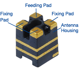
Figure 1: Chip antenna and its PCB footprint
The chip antenna, shown in Figure 1, contains one feeding pad, three fixing pads, and an antenna radiator. Let’s discuss these components in more detail:
- Feeding Pad: feeds the signal from the transmission line on the PCB
- Fixing Pad: three surface-mounted dummy pads are on the antenna to attach it to the PCB
- Antenna Radiator: a transducer to convert unguided RF waves to guided RF waves, and vice-versa
Important Board Level Guidelines for Chip Antenna Placement
The ground layer below the antenna affects the signal propagation and antenna radiation patterns. Therefore, it is not recommended to place the antenna above the ground plane. Figure 2 shows the correct position of the antenna. To avoid the electromagnetic interference from high-frequency components such as clock generators and other ICs, the antenna must be placed at the edge of the PCB with sufficient clearance from the rest of the circuit.
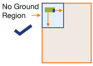
Figure 2: Optimal place to locate a chip antenna is in the no-ground region of the PCB.
The RF modem circuit is usually roofed by a metallic shielding container. If the antenna is placed very close to the shielding, the antenna radiation can be affected. Enough clearance from the shielding is required, as shown in Figure 3.
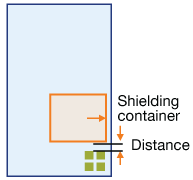
Figure 3: Distance for shielding container
Batteries are opaque to RF waves and can degrade the radiation efficiency, depending upon their size. As such, there must be adequate clearance between a chip antenna and the battery.
It is not recommended to put an LCD panel or speaker near the antenna section because they produce electromagnetic interference and can impact antenna performance. It is also recommended to place the impedance matching network, antenna, and radio output as close to each other as possible. This ensures a low signal loss from the chip antenna. We will discuss impedance matching in the next section.
Impedance Matching
For maximum power transfer and optimal performance of a chip antenna, the impedance of the antenna and transmission line must be matched. A typical matching circuit consists of a network of capacitors and inductors near the antenna. A few options are shown in Figure 4. Placement and orientation of the matching components are very important as they affect the magnetic field, which can couple with other components and can generate RF noise.
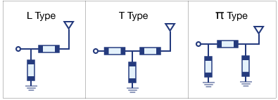
Figure 4: Matching Circuit Options
Antenna Performance Measurement
A measurement set up using a Vector Network Analyzer, as shown in Figure 5, is used to measure the performance of a chip antenna along with the matching circuit. We measure antenna parameters such as return loss, peak gain, efficiency, input impedance, and polarization at various feasible mounting locations.
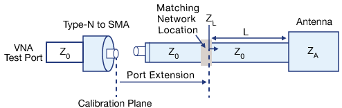
Figure 5: Antenna Matching Setup
The following are steps are taken into consideration when matching antenna impedance with a transceiver:
- Calibrate the vector network analyzer (VNA) as close to the matching network as possible
- Align the measurement plane with the calibration plane by using a port extension, if necessary
- Measure the unmatched impedance at the frequency used
- Decide the values of matching network components and incorporate the components
- Verify the matched impedance, and adjust, if needed
Ground Plane
The ground plane is a conductive horizontal surface which is a part of the antenna used to reflect the radio waves. Its length/width should be close to a quarter of the wavelength. An essential recommendation for the ground plane is that it should be continuous in any RF design. A discontinuous ground plane under the RF circuit makes the current return paths longer; this will affect the performance. With a continuous ground plane, a single via is sufficient to ground the pad, and we do not need to make an additional trace from pad to ground. The unused area on the top component plane should be filled with the ground plane and connected with the ground layer by many vias. The space between the vias must be about 1/10th of the wavelength.
Board Layers
An RF PCB can be designed on a two-layer or a four-layer PCB.
In a two-layer PCB board, the bottom layer is used as the ground plane, which provides the shortest path for return currents. Components and signal routing are placed on the top layer. The trace width is proportionate to PCB thickness. The PCB thickness must not be more than 0.8 mm to 1.0 mm to avoid unusual trace width. Higher trace width increases board area, while the lower thickness of a PCB makes it fragile. In complex routing, the trace length can become large and can be a part of RF radiation, which is undesirable.
In a 4-layer PCB design, separate layers are dedicated to ground and power. The recommended layer structure is:
- 1st Layer: Component and Signal
- 2nd Layer: Ground Plane
- 3rd Layer: Power Plane
- 4th Layer: Ground Plane and Signal Routing
A 4-layer design makes decoupling of the power plane placed between the ground plane and bottom layer easier.
RF Transmission Line
The transmission line is a pair of traces on a PCB having the desired characteristic impedance. We must design PCB traces very carefully for radio frequencies because the physical length of the PCB traces becomes a significant fraction of the wavelength. The impedance of a PCB trace is affected by its thickness, trace height above the ground plane, and PCB dielectric material. The impedance of the trace is critical to transfer maximum power out from the filter to the antenna. It is suggested to design the transmission line between the filter section and the antenna carefully.
There are different methods of creating the RF transmission line, namely Microstrip, suspended Stripline, and Coplanar Waveguide.
- Microstrip: consists of fixed-width metal routing along with a solid unbroken ground plane. This transmission line has low to high radiation. It supports 20- to 120-ohm characteristic impedance and a Q-factor of about 250. The PCB uses FR-4 dielectric substrate for microstrip-based etching due to its low cost.
- Suspended Stripline: contains a fixed-width routing on an inner layer, with solid ground planes above and below the center conductor. The conductor can be located in the center between the ground planes. This type of transmission line has low radiation. The characteristic impedance varies from 40 to 150 ohms, and the Q-factor is about 500.
- Coplanar Waveguide: delivers better isolation between nearby RF lines, as well as other signal lines. This medium involves a center conductor with ground planes on either side. This type of transmission line has medium radiation. It supports a Q-factor of 150, and characteristic impedance varies from 20 to 250.
Transmission Line Bends and Corner Compensation
When we change the direction of the transmission lines due to routing limitations, we must use a bend radius which is more than three times that of the center conductor width to avoid any change in characteristic impedance.
When a gradually curved bend is not possible, we make a right-angle bend by increasing the effective line width and reducing the impedance discontinuity. A 90-degree bend in a transmission line adds some capacitance. A mitered bend, (i.e., a fish-head-shaped joint of two rectangular pieces), as shown in Figure 6, chops off some capacitance and restores the line to its original characteristic impedance.
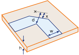
Figure 6: Transmission Line bend
Power Supply Bypassing and Decoupling
High-frequency noise on the PCB can travel to the supply pins of the device. Proper power signal routing with de-coupling and bypass capacitors helps to reduce this noise. It is recommended to use a capacitor on the supply pin of the device to bypass the high-frequency harmonics to ground. The digital signals on the board are fast switching rail to rail, and generate high-frequency noise. These harmonics can couple with the power supply line and affect the performance. It is recommended that the power supply line is decoupled and routed away from the RF part area on the PCB.
Chip Antenna Simulation
Various Evaluation Kits (EVK) are available to demonstrate the RF simulation for a chip antenna with the recommended circuit design. The EVK includes a chip antenna mounted on a specified size of the printed circuit board, with an RF (SMA) launch connector for transmission or reception of signal. PCB Design Tools and Software also help in simulating the tuning circuits as they would perform with the layout before fabrication. It helps to optimize the number of re-spins of the PCB to arrive at the final desired performance.
Top Comments
-

DAB
-
Cancel
-
Vote Up
+4
Vote Down
-
-
Sign in to reply
-
More
-
Cancel
Comment-

DAB
-
Cancel
-
Vote Up
+4
Vote Down
-
-
Sign in to reply
-
More
-
Cancel
Children