element14 Community
element14 Community
    Register Log In
  • Site
  • Search
  • Log In Register
  • About Us
  • Community Hub
    Community Hub
    • What's New on element14
    • Feedback and Support
    • Benefits of Membership
    • Personal Blogs
    • Members Area
    • Achievement Levels
  • Learn
    Learn
    • Ask an Expert
    • eBooks
    • element14 presents
    • Learning Center
    • Tech Spotlight
    • STEM Academy
    • Webinars, Training and Events
    • Learning Groups
  • Technologies
    Technologies
    • 3D Printing
    • FPGA
    • Industrial Automation
    • Internet of Things
    • Power & Energy
    • Sensors
    • Technology Groups
  • Challenges & Projects
    Challenges & Projects
    • Design Challenges
    • element14 presents Projects
    • Project14
    • Arduino Projects
    • Raspberry Pi Projects
    • Project Groups
  • Products
    Products
    • Arduino
    • Avnet Boards Community
    • Dev Tools
    • Manufacturers
    • Multicomp Pro
    • Product Groups
    • Raspberry Pi
    • RoadTests & Reviews
  • Store
    Store
    • Visit Your Store
    • Choose another store...
      • Europe
      •  Austria (German)
      •  Belgium (Dutch, French)
      •  Bulgaria (Bulgarian)
      •  Czech Republic (Czech)
      •  Denmark (Danish)
      •  Estonia (Estonian)
      •  Finland (Finnish)
      •  France (French)
      •  Germany (German)
      •  Hungary (Hungarian)
      •  Ireland
      •  Israel
      •  Italy (Italian)
      •  Latvia (Latvian)
      •  
      •  Lithuania (Lithuanian)
      •  Netherlands (Dutch)
      •  Norway (Norwegian)
      •  Poland (Polish)
      •  Portugal (Portuguese)
      •  Romania (Romanian)
      •  Russia (Russian)
      •  Slovakia (Slovak)
      •  Slovenia (Slovenian)
      •  Spain (Spanish)
      •  Sweden (Swedish)
      •  Switzerland(German, French)
      •  Turkey (Turkish)
      •  United Kingdom
      • Asia Pacific
      •  Australia
      •  China
      •  Hong Kong
      •  India
      •  Korea (Korean)
      •  Malaysia
      •  New Zealand
      •  Philippines
      •  Singapore
      •  Taiwan
      •  Thailand (Thai)
      • Americas
      •  Brazil (Portuguese)
      •  Canada
      •  Mexico (Spanish)
      •  United States
      Can't find the country/region you're looking for? Visit our export site or find a local distributor.
  • Translate
  • Profile
  • Settings
Community Hub
Community Hub
Member Blogs Experimenting with MOSFETS: Total Gate Charge
  • Blog
  • Forum
  • Documents
  • Quiz
  • Events
  • Leaderboard
  • Polls
  • Files
  • Members
  • Mentions
  • Sub-Groups
  • Tags
  • More
  • Cancel
  • New
Join Community Hub to participate - click to join for free!
  • Share
  • More
  • Cancel
Group Actions
  • Group RSS
  • More
  • Cancel
Engagement
  • Author Author: jc2048
  • Date Created: 2 Aug 2019 11:38 AM Date Created
  • Views 6401 views
  • Likes 6 likes
  • Comments 14 comments
  • mosfet
  • test
  • gate charge
  • constant current
  • jfet
  • mfet
  • jc2048
Related
Recommended

Experimenting with MOSFETS: Total Gate Charge

jc2048
jc2048
2 Aug 2019

Introduction


More experimenting, this time with MOSFETs.


If you've ever designed with a MOSFET, I'm sure you've seen the kind of curves that are usually present in the datasheet showing the relationship between the total gate charge and the gate voltage. Here's one such graph from a datasheet for a Vishay IRF730 device:


image

They always have the same sort of shape to the curve, though the position of the plateau, halfway up, varies in both voltage and the amount of charge to get there, and then past it, for a particular type of part.


The IRF730 is a power MOSFET. As a comparison, here's the curve for a small-signal 2N7000 part (from a Fairchild datasheet)


image

For this part, the charge values are much lower.


The reason I'm showing you these curves is that I thought I could have a go at measuring one for myself.


I'm going to try measuring the one for the IRF730. I want to see if I can do a reasonable measurement of this using just simple equipment - the equipment I've used here being an oscilloscope, a bench multimeter, and a current probe for setting the drain current. [The reason for using the current probe was that the current is only present for 10uS. Setting it at dc with the bench meter was out because of how hot the device quickly gets - the reading over 10uS would then be nothing like the value set at dc.]


The reason I chose the IRF730 is that the charge values will allow for a test over about 10us with a gate current of a few milliamps. I decided that was more manageable than for the small-signal parts where either the gate current would need to be much lower or the test would have to be run very much more quickly. Although the IRF730 is a power device, the current figures are quite modest because it's intended for high-voltage work. The bench supply I'm going to use for the Vds supply can only mange 0-30V at 0-3A so, with the IRF730, the curves I get will be more in line with the datasheet ones than they would be if I chose a lower-voltage device operated at 50A, or whatever.

I'm also curious as to whether the curve really comes out that good or whether there's a little artistic licence there. Did someone get their ruler out and tidy up the curves? I'm sure they didn't, but I'd like to see for myself.


The Circuit


The circuit I've ended up with is based on the ones shown on datasheets. They vary somewhat, but the essentials seem to remain the same between the different manufacturers. The drain current is normally supplied by a similar part to the one on test, configured to deliver a constant current. The gate drive for that part has to be relative to its source which sits on the drain of the device under test and will move up and down. To deal with that, I decided to simply use a 9V battery to generate the gate voltage. I imagine the reason for using a similar part to the one on test is so that the timing matches and they start as quickly as each other. Also, their capabilities will match in terms of current and breakdown voltage, etc.


The gate drive for the device under test necessitated a little bit of simple design. Datasheet circuits usually just show a current generator, which is fine if you are a semiconductor manufacturer with cabinets full of test equipment but I don't have that so I'm going to have to make one. It needs to respond reasonably fast, so rather than use an op-amp I decided to try a JFET. I had some BF256BBF256B n-channel parts, so used one of those - here's how it's configured.


image


The potentiometer allows the gate to be set to a negative voltage relative to the source. The zero-volts current was just over 8.6mA, but I adjusted the pot down from there to give a fairly precise 'round figure' of 5mA in order to make the time display on the oscilloscope relate nicely to the charge value. In terms of charge delivery, that will be 5nC per microsecond.


Here's the full circuit


image


For controlling the timing of the test, I used an Arduino Uno. The program sets pin 12 high for 10us and then low for 500us, a 2% duty cycle. I turned off interrupts whilst it was high so that the timing interval would be consistent. The long off period means the test can be done with reasonably high drain currents and drain voltages, up to 3A and 30V (giving a maximum instantaneous power of 90W), without heat dissipation in the MOSFETs being too much of an issue.

When pin 12 is low (or if the Arduino is either powered off or not connected), the first transistor is off, the second transistor is on and the gate current is directed to ground leaving the Vgs of the test part close to zero and the DUT off, with more or less zero gate charge. When pin 12 goes high, the constant current is then redirected to the gate. The oscilloscope triggers at the same point. From that point on, the display is then equivalent to 5nC per microsecond and if I apply a probe to measure the gate voltage we should see the same curve plotted as on the datasheet.


Here's the test circuit built on a scrap of pcb material.


image


Doing Some Tests


Before I start experimenting with the MOSFET, I'm going to try running the constant current into a 4.7nF capacitor [measured 4.77uF] in place of the MOSFET gate. If it works, I should see a linear ramp as it charges up to about 10.5V at the end of the 10uS. Here's the trace I got - the yellow trace is the signal from the Uno controlling the test.


image


That looks quite reasonable. Not quite straight, but good enough for what I'm doing for this blog.


This next trace is with the current applied to the gate of the test part. The drain current is set to 1A and the drain voltage to 10V. The yellow trace is the 10uS pulse from the Arduino, the blue trace is Vgs.


image


That nicely shows the shape of the Vgs voltage versus the total gate charge curve. Ignore the top end when the Vgs gets above 15V - that's the FET constant-current generator starting to fail as it runs out of voltage.


This next one shows the Vgs again, and this time the yellow trace shows the drain voltage and how it falls as the transistor turns on.


image


Each division across is 2nC, so the plateau starts just under 3.5nC, which ties up with the datasheet. The Vgs is much lower though - theirs is around 6V, whereas mine is just over 4V. A little of the difference is down to the drain current - this curve is for 1A, whereas theirs is for 3.5A - but mostly it's just a reflection of the wide variation in threshold voltage.


The end of the plateau is quite different in my case - mine stops at around 10nC - but that's for a Vds of only 10V. Their curves are for much higher drain voltages.


Next experiment was to vary the drain current and see what effect it has on the charge curve


image


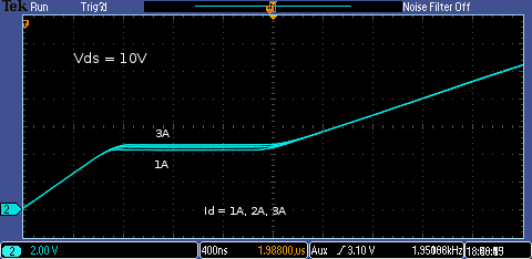
The effect is quite subtle, but It lifts the plateau a small amount as the current increases.


Now, here's what happens if I keep the current at 1A and change Vds.


image


I was pleased with all those. Sometimes experimenting doesn't go very well, but this time it worked quite nicely.


Although I'm mostly just replicating what's on the datasheet, it has given me a better appreciation of how the Vgs versus total gate charge curve changes with drain voltage and drain current. Sometimes datasheets just show a curve taken with a single value for each which hides from you the effect of changing either if you're not too familiar with how the devices work.


If you found this interesting and would like to see more blogs I've written, a list can be found here: jc2048 Blog Index

  • Sign in to reply

Top Comments

  • colporteur
    colporteur over 6 years ago +2
    Nice work. Sean
  • jc2048
    jc2048 over 6 years ago +2
    Although I didn't mention it in the blog above, when I first tried the experiment I got something wrong. Without thinking too much about what I was doing, I added a gate resistor of 100 ohms in series…
  • dougw
    dougw over 6 years ago +2
    Very nicely done...cool experiment. When I saw the title, I though oh ya they do have some weird characteristic. I don't normally think too much about such things, but I find them interesting. I'm glad…
  • jc2048
    jc2048 over 6 years ago in reply to colporteur +1
    Thank you.
  • genebren
    genebren over 6 years ago +1
    Very cool experiment/demonstration. It is nice when thing go well, as seen in this setup.
  • jc2048
    jc2048 11 months ago in reply to maxjack123 +1
    The idea for this blog originally came from the datasheet itself, where they show this test circuit. I simply took that and fleshed it out. The top transistor is acting as a floating current source…
Parents
  • ellen86119
    ellen86119 over 1 year ago

    I used the same method as you for the current source, but my current source was a little slow to respond.

    It takes 20us to reach the 5mA I set.

    JFET(LSK170B)image

    • Cancel
    • Vote Up 0 Vote Down
    • Sign in to reply
    • More
    • Cancel
  • jc2048
    jc2048 over 1 year ago in reply to ellen86119

    Hello. Thanks for reading the blog. It was a long time back and I don't remember it very well.

    Am I understanding your circuit properly? Q2 takes the place of the bipolar transistor I was using to redirect the current to ground until the start of the test?

    How are you measuring the current? If you're looking at the voltage on the 1k2 and calculating, at the start it will be affected by the drain capacitance of Q2 charging to the steady-state 1V you'd expect to see across the 1k2.

    • Cancel
    • Vote Up 0 Vote Down
    • Sign in to reply
    • More
    • Cancel
  • ellen86119
    ellen86119 over 1 year ago in reply to jc2048

    Yes, I used Q2 takes the place of the bipolar transistor. Using to redirect the current to ground until the start of the test.

    I used a 1k2 resistor to check the current source response. I look at the voltage on the 1k2 and calculate the current. The response speed of the current source may be affected by the drain capacitance of Q2. I will confirm whether this affects it, so the Datasheet uses bipolar transistor instead of MOSFET.

    • Cancel
    • Vote Up 0 Vote Down
    • Sign in to reply
    • More
    • Cancel
  • jc2048
    jc2048 over 1 year ago in reply to ellen86119

    This is the kind of thing a datasheet shows. This is for an IRF730 from Vishay.

    image

    It's quite schematic (bare bones). No indication of what is generating the current for the gate.

    I think one reason that they originally used to show these might have been that many of the MOSFET parameters we use in design aren't intrinsic but depend on how they are measured and the conditions of measurement, and this was a way to emphasise that to the many designers who were new to MOSFETs.

    My circuit with the JFET, as a current source, and a bipolar transistor, to steer the current, was an attempt to do something equivalent without using the kind of expensive test equipment that the manufacturer would use. It isn't necessarily very good and could almost certainly be improved, but it is a way to get an indicative look at what is happening with the gate charge.

    As long as all your wiring is short (low inductance) and you haven't accidentally left the scope set to a bandwidth of 100kHz, then there are several possibilities.

    My first thought was output capacitance of the MOSFET (it's going to be larger than the 4pF max of the RF bipolar transistor), however, problem here is that (roughly) 50nF (C = i x dt/dv) is an extremely high (and improbable) value, even for a large power device.

    Another problem area might be the drive to your MOSFET. If that comes from a generator then you've got 50 ohms in series with the internal gate resistance (maybe another 50R), but that only gives a time constant of 100ns, even with the high input capacitance of a power device, so manybe that's a dead end too.

    So that leaves us back with the JFET sourcing the current. In your circuit it has to try and cope with the 1V step-change in voltage that your current measuring asks for and fails. It might be that my BF part (originally designed for RF use) could do better than a part designed to be good for audio use, but I suspect it would behave much the same - the part you've chosen looks like it would be pretty fast (low intrinsic capacitances). If you have to measure the current like that, I think you need to design a faster source.

    • Cancel
    • Vote Up 0 Vote Down
    • Sign in to reply
    • More
    • Cancel
  • jc2048
    jc2048 over 1 year ago in reply to jc2048

    Correction: where I said a 1V step, I should have said 6V. 5mA x 1.2k = 6V.

    If I simulate what you're doing with a BF256B for the source and a 2N7000 for the switching device, I get this

    image

    image

    the simulator won't get everything right but will be fairly close. 200ns is a lot different to your 20us.

    If I substitute an IRF520 power device for the 2N7000 small-signal part, it is slower, but even there it only takes just over 1uS.

    At this point I've run out of ideas. If you work your way around, considering each thing in turn, you should be able explain what's going on.

    • Cancel
    • Vote Up 0 Vote Down
    • Sign in to reply
    • More
    • Cancel
  • ellen86119
    ellen86119 over 1 year ago in reply to jc2048

    Sorry, I missed the message. I tried changing the MOS, from Power MOS to Small signal MOS. The response speed of the current source is significantly faster. But when I compared the data in the datasheet, there was not much difference between Coss. There is a big difference in Ciss, but in theory it should not have any impact. I might try it experimentally to confirm which parameter of the MOS affects the current response speed.

    Power MOS:IPA70R360P7XKSA1

    Small signal MOS:2N7002NXAKR

    image

    • Cancel
    • Vote Up 0 Vote Down
    • Sign in to reply
    • More
    • Cancel
  • jc2048
    jc2048 over 1 year ago in reply to ellen86119

    Looks like I was wrong to be focussing so much on the output capacitance.

    Doesn't this then take us back to the thing you were originally looking at - the gate charge?

    When the MOSFET turns off, you have to remove much of the charge from the gate for that to happen. If your gate drive does that at a constant rate (probably not true, but maybe a very rough approximation initially?), then the IPA70R360 is going to take ten times longer than the 2N70002 (compare the total gate charge curves for both).

    Although that's not quite the same thing as the input capacitance, the two are very closely related and the input capacitance is indicative of what you're going to find with the gate charge (up to the threshold, the gate charge is simply what is needed to charge that capacitance between the gate and the source to get the gate voltage up).

    • Cancel
    • Vote Up 0 Vote Down
    • Sign in to reply
    • More
    • Cancel
Comment
  • jc2048
    jc2048 over 1 year ago in reply to ellen86119

    Looks like I was wrong to be focussing so much on the output capacitance.

    Doesn't this then take us back to the thing you were originally looking at - the gate charge?

    When the MOSFET turns off, you have to remove much of the charge from the gate for that to happen. If your gate drive does that at a constant rate (probably not true, but maybe a very rough approximation initially?), then the IPA70R360 is going to take ten times longer than the 2N70002 (compare the total gate charge curves for both).

    Although that's not quite the same thing as the input capacitance, the two are very closely related and the input capacitance is indicative of what you're going to find with the gate charge (up to the threshold, the gate charge is simply what is needed to charge that capacitance between the gate and the source to get the gate voltage up).

    • Cancel
    • Vote Up 0 Vote Down
    • Sign in to reply
    • More
    • Cancel
Children
No Data
element14 Community

element14 is the first online community specifically for engineers. Connect with your peers and get expert answers to your questions.

  • Members
  • Learn
  • Technologies
  • Challenges & Projects
  • Products
  • Store
  • About Us
  • Feedback & Support
  • FAQs
  • Terms of Use
  • Privacy Policy
  • Legal and Copyright Notices
  • Sitemap
  • Cookies

An Avnet Company © 2025 Premier Farnell Limited. All Rights Reserved.

Premier Farnell Ltd, registered in England and Wales (no 00876412), registered office: Farnell House, Forge Lane, Leeds LS12 2NE.

ICP 备案号 10220084.

Follow element14

  • X
  • Facebook
  • linkedin
  • YouTube