element14 Community
element14 Community
    Register Log In
  • Site
  • Search
  • Log In Register
  • Community Hub
    Community Hub
    • What's New on element14
    • Feedback and Support
    • Benefits of Membership
    • Personal Blogs
    • Members Area
    • Achievement Levels
  • Learn
    Learn
    • Ask an Expert
    • eBooks
    • element14 presents
    • Learning Center
    • Tech Spotlight
    • STEM Academy
    • Webinars, Training and Events
    • Learning Groups
  • Technologies
    Technologies
    • 3D Printing
    • FPGA
    • Industrial Automation
    • Internet of Things
    • Power & Energy
    • Sensors
    • Technology Groups
  • Challenges & Projects
    Challenges & Projects
    • Design Challenges
    • element14 presents Projects
    • Project14
    • Arduino Projects
    • Raspberry Pi Projects
    • Project Groups
  • Products
    Products
    • Arduino
    • Avnet & Tria Boards Community
    • Dev Tools
    • Manufacturers
    • Multicomp Pro
    • Product Groups
    • Raspberry Pi
    • RoadTests & Reviews
  • About Us
    About the element14 Community
  • Store
    Store
    • Visit Your Store
    • Choose another store...
      • Europe
      •  Austria (German)
      •  Belgium (Dutch, French)
      •  Bulgaria (Bulgarian)
      •  Czech Republic (Czech)
      •  Denmark (Danish)
      •  Estonia (Estonian)
      •  Finland (Finnish)
      •  France (French)
      •  Germany (German)
      •  Hungary (Hungarian)
      •  Ireland
      •  Israel
      •  Italy (Italian)
      •  Latvia (Latvian)
      •  
      •  Lithuania (Lithuanian)
      •  Netherlands (Dutch)
      •  Norway (Norwegian)
      •  Poland (Polish)
      •  Portugal (Portuguese)
      •  Romania (Romanian)
      •  Russia (Russian)
      •  Slovakia (Slovak)
      •  Slovenia (Slovenian)
      •  Spain (Spanish)
      •  Sweden (Swedish)
      •  Switzerland(German, French)
      •  Turkey (Turkish)
      •  United Kingdom
      • Asia Pacific
      •  Australia
      •  China
      •  Hong Kong
      •  India
      •  Japan
      •  Korea (Korean)
      •  Malaysia
      •  New Zealand
      •  Philippines
      •  Singapore
      •  Taiwan
      •  Thailand (Thai)
      •  Vietnam
      • Americas
      •  Brazil (Portuguese)
      •  Canada
      •  Mexico (Spanish)
      •  United States
      Can't find the country/region you're looking for? Visit our export site or find a local distributor.
  • Translate
  • Profile
  • Settings
Community Hub
Community Hub
Member's Forum Learning FPGA
  • Blog
  • Forum
  • Documents
  • Quiz
  • Events
  • Leaderboard
  • Polls
  • Files
  • Members
  • Mentions
  • Sub-Groups
  • Tags
  • More
  • Cancel
  • New
Join Community Hub to participate - click to join for free!
Actions
  • Share
  • More
  • Cancel
Forum Thread Details
  • Replies 15 replies
  • Subscribers 615 subscribers
  • Views 535 views
  • Users 0 members are here
  • fpga
Related

Learning FPGA

danielpgleason
danielpgleason 23 days ago

Does anyone know of any good learning resources about how to start learning FPGA? I've been a software engineer for several years and the FPGA world is quite new to me. I'm trying to implement RMII but have been struggling a lot. I purchased a logic analyzer but I don't know what I'm looking at. I need something that will tell me how to properly understand and read datasheets, know how to debug signals, how to understand what VHDL is good and what is bad. How to read RTL generations..Etc

I'm starting from the beginning. Any resources or materials are greatly appreciated. 

  • Sign in to reply
  • Cancel
  • veluv01
    veluv01 14 days ago

    Since you're getting into FPGA's as an software engineer, I assume you're familiar with C/C++; I highly recommend  the HLS based approach for configuring the FPGA using Vitis Unified IDE.(AMD FPGA tools)

    AMD provides good docs for HLS based design flow

    https://docs.amd.com/r/en-US/ug1399-vitis-hls/Introduction

    https://docs.amd.com/r/en-US/ug1399-vitis-hls/HLS-Programmers-Guide

    HLS based approach saves you a lot of time and you can just use the ILA IP to debug the design instead of using the Logic Analyser.

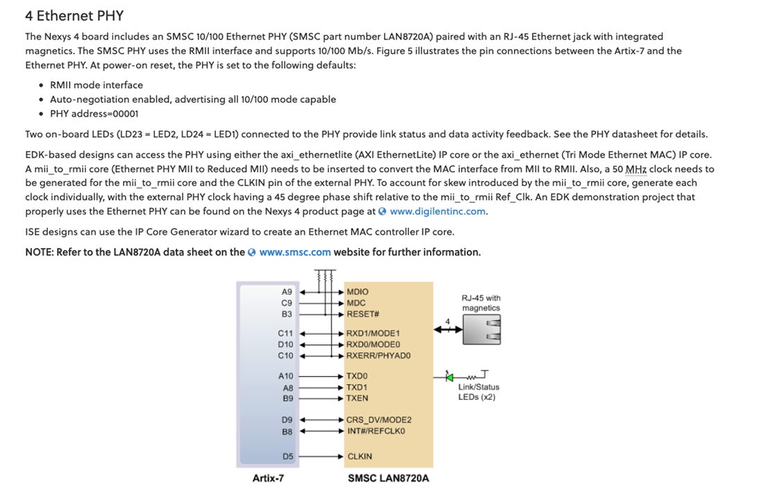
    For the FPGA....I would suggest going with NEXYS 4, the documentation is good and it's PL got an Ethernet PHY with RMII ; perfect for you.

    image

    Here's a best video reference for the FPGA and  Ethernet

    https://www.youtube.com/watch?v=78tkdc6Lq_8

    • Cancel
    • Vote Up 0 Vote Down
    • Sign in to reply
    • Cancel
  • Moussa1492
    Moussa1492 14 days ago

    A good path would be:

    1. Start with FPGA fundamentals

    For a software engineer, the biggest mindset shift is:

    VHDL/Verilog is not “code that runs.”
    It describes hardware that exists all the time.

    Good beginner resources:

    Resource Why it helps
    Nandland FPGA / VHDL / Verilog tutorials Very beginner-friendly, especially if you are coming from software. It has FPGA-101, VHDL, and Verilog sections. (Nandland)
    VHDLwhiz Basic VHDL Course Good if you want VHDL specifically. It starts in simulation, so you can learn without fighting hardware first. (VHDLwhiz)
    MIT 6.111 Introductory Digital Systems Lab More academic, but excellent for understanding digital systems, timing, state machines, and hardware design thinking.
    Digilent FPGA digital design materials Good if you use common dev boards like Basys, Nexys, Arty, etc. Their material focuses on hands-on FPGA projects. (Digilent)

    Start with small designs:

    LED blink
    button debounce
    counter
    UART transmitter
    UART receiver
    FIFO
    simple SPI master
    simple packet parser
    

    Do not start with Ethernet.


    2. Learn simulation before hardware debugging

    Before using a logic analyzer, learn to use a simulator:

    • GHDL / Questa / ModelSim for VHDL

    • Verilator / Icarus / Questa for Verilog/SystemVerilog

    • GTKWave for waveform viewing

    You should be able to answer:

    What signal changed?
    On which clock edge?
    Was reset active?
    Was this register updated now or next cycle?
    Is this combinational or sequential logic?
    

    A very good FPGA workflow is:

    Write RTL
    ↓
    Write testbench
    ↓
    Simulate
    ↓
    Check waveforms
    ↓
    Synthesize
    ↓
    Check RTL/netlist schematic
    ↓
    Constrain timing
    ↓
    Program FPGA
    ↓
    Debug with internal logic analyzer
    

    For “how to read RTL generation,” use the vendor schematic/netlist viewer after synthesis. In Vivado, for example, design analysis is specifically meant to inspect optimized netlists and timing results. (Xilinx)


    3. Learn what “good RTL” means

    Good FPGA RTL usually means:

    -- Good mental model
    one clock
    synchronous reset or controlled reset
    registered outputs
    clear state machines
    no accidental latches
    no gated clocks
    no random delays
    clean clock-domain crossing
    

    Bad beginner RTL usually has:

    multiple unrelated clocks everywhere
    using delays like wait for 10 ns in synthesizable logic
    incomplete if/case statements causing latches
    combinational feedback
    gated clocks
    async signals used directly
    ignoring timing constraints
    

    Clock-domain crossing is especially important. Xilinx-style HDL guidelines warn against asynchronous design techniques and recommend proper methods such as FIFOs when crossing clock domains. (Wiki des Electroniciens du CNRS)

    For timing and CDC, read:

    Topic Resource
    Clock-domain crossing 01signal CDC articles (01signal)
    Timing closure 01signal timing closure series (01signal)
    Debug/formal later ZipCPU tutorials — very good after you know the basics, especially for debugging and formal verification. (ZipCPU)

    4. For RMII specifically: learn the interface first

    RMII is not just “some pins.” It is a synchronous interface around a 50 MHz reference clock.

    Typical RMII signals:

    Signal Direction Meaning
    REF_CLK clock 50 MHz reference clock
    TX_EN MAC → PHY transmit data valid
    TXD[1:0] MAC → PHY 2-bit transmit data
    CRS_DV PHY → MAC carrier sense / receive data valid
    RXD[1:0] PHY → MAC 2-bit receive data
    RX_ER PHY → MAC receive error, sometimes optional
    MDC/MDIO management PHY register access

    Microchip’s KSZ8081 datasheet states that REF_CLK is a continuous 50 MHz clock used as the timing reference for TXEN, TXD[1:0], CRS_DV, RXD[1:0], and RX_ER. (Microchip)

    So the first question is not “is my VHDL correct?” The first questions are:

    Is the PHY strapped into RMII mode?
    Is the 50 MHz REF_CLK present?
    Who generates REF_CLK: FPGA, PHY, or oscillator?
    Can I read the PHY ID over MDIO?
    Does the PHY report link up?
    Is reset released correctly?
    Are the I/O voltages correct?
    

    TI’s DP83848 RMII application note also says RMII mode requires a 50 MHz external CMOS oscillator source and correct strap configuration at reset. (Texas Instruments)


    5. Your logic analyzer may not be enough

    RMII runs at 50 MHz. If your logic analyzer is a cheap 24 MHz or 50 MHz USB analyzer, it will not reliably show RMII data.

    For RMII, use:

    External logic analyzer:
    - reset
    - strap pins
    - MDC/MDIO
    - link LEDs
    - slow control signals
    
    FPGA internal logic analyzer:
    - RMII RXD/TXD
    - TX_EN
    - CRS_DV
    - state machines
    - FIFOs
    - packet parser signals
    

    For Xilinx, use ILA.
    For Intel/Altera, use SignalTap.
    For Lattice, use the available internal debug flow depending on the toolchain.

    A practical RMII capture should trigger on:

    TX_EN rising edge
    or
    CRS_DV rising edge
    

    Then inspect:

    REF_CLK stable at 50 MHz
    TX_EN high during transmit frame
    TXD[1:0] changing only relative to REF_CLK
    CRS_DV high during received frame
    RXD[1:0] changing during CRS_DV
    

    6. Debug RMII in layers

    Do not debug the whole Ethernet stack at once.

    Use this order:

    Layer 1 — PHY alive

    Check:

    PHY reset pin
    PHY clock
    PHY straps
    PHY address
    MDIO read works
    PHY ID registers readable
    link status readable
    

    If MDIO does not work, stop. Do not debug RMII yet.

    Layer 2 — transmit only

    Make FPGA send a simple Ethernet frame repeatedly.

    Look for:

    TX_EN goes high
    TXD[1:0] toggles
    PHY shows activity
    PC/Wireshark sees something
    

    Layer 3 — receive only

    Send broadcast traffic from a PC:

    ARP
    ping
    broadcast packet
    

    Look for:

    CRS_DV goes high
    RXD[1:0] toggles
    your RX state machine detects preamble/SFD
    

    Layer 4 — MAC framing

    Only after the electrical/interface side works, worry about:

    preamble
    SFD
    destination MAC
    source MAC
    EtherType
    payload
    CRC/FCS
    inter-frame gap
    

    7. Suggested learning order for your case

    Given that you are already trying RMII, I would follow this path:

    Week 1:
    Learn VHDL simulation, clocked processes, testbenches, GTKWave.
    
    Week 2:
    Build UART TX/RX in simulation and on FPGA.
    
    Week 3:
    Learn FIFOs, valid/ready handshakes, simple packet streams.
    
    Week 4:
    Read PHY datasheet carefully: reset, straps, clocking, MDIO, RMII timing.
    
    Week 5:
    Implement MDIO read/write first.
    
    Week 6:
    Implement RMII TX only.
    
    Week 7:
    Implement RMII RX only.
    
    Week 8:
    Build a minimal Ethernet MAC: ARP or UDP only.
    

    Best immediate advice

    For your RMII struggle, focus on these three things first:

    1. Can you read the PHY ID over MDIO?
      If no, your hardware/configuration is not ready.

    2. Is REF_CLK definitely correct?
      RMII depends on a continuous 50 MHz clock. Wrong clock source or wrong PHY strap will break everything.

    3. Use internal FPGA logic analyzer, not only external LA.
      RMII is fast enough that many hobby logic analyzers will mislead you.

    A very good first goal is:

    Read PHY ID over MDIO
    ↓
    Confirm link up
    ↓
    Transmit one repeated raw Ethernet frame
    ↓
    See it in Wireshark
    

    Once that works, then build RX and higher-level protocol handling.

    • Cancel
    • Vote Up +2 Vote Down
    • Sign in to reply
    • Cancel
  • michaelkellett
    michaelkellett 14 days ago in reply to geralds

    Beware !

    This package from Elektor features VHDPlus not VHDL - please checkout VHDPlus very carefully before you go that route.

    If you want a cheap start there is plenty of free material on the web and you can buy some very low cost hardware for Altera chips from Aliexpress.

    MK

    • Cancel
    • Vote Up 0 Vote Down
    • Sign in to reply
    • Cancel
  • geralds
    geralds 15 days ago in reply to danielpgleason

    Hi,

    For example: you can try this kind of FPGA.

    https://www.elektor.de/products/fpga-programming-and-hardware-essentials

    This is a cheap tool and, in this book will be explained the essentials of FPGAs.

    • Cancel
    • Vote Up 0 Vote Down
    • Sign in to reply
    • Cancel
  • geralds
    geralds 21 days ago

    Hi  danielpgleason 

    I used to work with Lattice PLDs and FPGAs for over 10 years until 2013.

    The logic devices are simple in design, easy to learn, and quite inexpensive.

    You can find good literature on them at Lattice Semiconductor.

    https://www.latticesemi.com/

    You can program the PLDs and basic FPGAs with the downloadable, mostly free software.

    https://www.latticesemi.com/Products/DesignSoftwareAndIP/FPGAandLDS/ispLEVERClassic

    Use this software for the classic types, ispLSI, PLD, GAL. etc..

    https://www.latticesemi.com/Products/DesignSoftwareAndIP/FPGAandLDS/LatticeDiamond

    Use Diamond for programming as older types as well, e.g. MachXO; ECP2;


    https://www.latticesemi.com/Products/DesignSoftwareAndIP/FPGAandLDS/LatticePropel

    Use Propel for MACHXO4; 5; Certus; some older types - iCE40;... 


    https://www.latticesemi.com/Support/Licensing

    Altera and Xilinx (where I worked with the Spartan types) would also be options, however,
    these types are quite expensive, as are the devices necessary for their development.
    It's a bit hug for you, I think.

    For you:

    some simple question where be answered: what is a PAL, GAL, PLD (CPLD), FPGA, ASIC (historically increasing in complexity)?
    What can I do with it? Do you train with logical truth-tables? Metastability, logic-gates, registers, timing, etc...

    Regards,
    Gerald


    • Cancel
    • Vote Up +1 Vote Down
    • Sign in to reply
    • Cancel
  • danielpgleason
    danielpgleason 21 days ago in reply to AngelSoto

    I want to try to implement ethernet. 

    • Cancel
    • Vote Up 0 Vote Down
    • Sign in to reply
    • Cancel
  • AngelSoto
    AngelSoto 22 days ago

    Nice topic.

    I saw some VHDL at university a few years ago, but this discussion is definitely
    bringing back the need to learn more and refresh, or even update, my hands-on FPGA
    experience.

    As michaelkellett mentioned the Artix platform, I realized that it’s actually the same
    direction I’ve been looking at recently. I’m planning to buy an Artix development board
    soon and add it to my short-term project bucket list. In my case, it’s the Digilent
    Cmod A7 with the Xilinx Artix-7 FPGA.

    Funny timing, because this is exactly the kind of topic I’ve been thinking about
    getting into lately, so all the recommendations here are really useful.

    • Cancel
    • Vote Up 0 Vote Down
    • Sign in to reply
    • Cancel
  • dang74
    dang74 22 days ago

    This might be controversial but I think the best way to learn FPGA is not to jump into the HDL languages right away.  If you are using the Altera environment use their block diagram editor which allows you to string together logic gates and flip flops in a schematic.... but don't stop there... use their wizard to create parametrized counter and compare blocks.  You may have heard that unlike software, FPGAs are parallel.. well that is true, but you can create sequences by decoding count values (of a clocked counter) for instance... or you can have a series of interdependent clocked registers that only advance when certain conditions occur.  I would spend a month to see what can be accomplished with counters, gates and compare blocks before moving to HDL.  The behavior of your designs can be tested using ModelSim (which I assume is still packaged with their software) or if you are working with a development board on Signal Tap II (their embedded logic analyzer) 

    • Cancel
    • Vote Up +1 Vote Down
    • Sign in to reply
    • Cancel
  • michaelkellett
    michaelkellett 22 days ago in reply to michaelkellett

    Just remembered, one of the examples that comes with the Microphase Artix dev board (see third link above) has a bare metal to RMII interface.

    This is NOT the place to start learning about FPGAs  - try something simpler first.

    SPI is much, much easier.

    MK

    • Cancel
    • Vote Up 0 Vote Down
    • Sign in to reply
    • Cancel
  • michaelkellett
    michaelkellett 22 days ago in reply to danielpgleason

    Altera FPGAs are well documented and at the lower and simpler end have some advantages over AMD/Xilinx.

    They have a wider range of low end parts and some of these are available on very attractively priced dev boards. There are many Altera FPGAs still available in TQFP packages which makes the attractive for low cost prototyping.

    For a complete beginner I would recommend Lattice or Efinix FPGAs.

    Small Lattice FPGAs are cheap and very cheap dev boards are avaialble. The Lattice tools and workflow for the simple chips is much easier to get started with than Altera or Xilinx. If you care about this there are Open Source tools for the small Lattice chips (I haven't used them so can't comment on ease of use.)

    I find the Efinix chips to be good cheap and the tools OK but harder work than Lattice.

    Another option is Gowin, very cheap boards, very cheap parts if you want to but  a lot but less easy tools.

    Here's a really cheap Altera baord, lot smore on Aliexpress and you will need  a "Byte Blaster" to program it. You can download the Altera tools for free..

    https://www.aliexpress.com/item/1005008090630134.html

    Here's a Lattice board with an Ethernet port and a rather bigger Lattice FPGA. The iceNano boards are maybe easier to get started with but cost more for a lot less FPGA. You will need a programmer for the ECP based board.

    https://www.aliexpress.com/item/1005008611836768.html

    This is quite a nice Xilinx board (an I've actually bought and used these and they are quite good - documentation and support is OK, not brilliant, bet you can get schematics and examples that work (you will need to use a translator on the comments in the examples unless you can read Chinese))

    https://www.aliexpress.com/item/1005005252087623.html

    MK

    • Cancel
    • Vote Up +2 Vote Down
    • Sign in to reply
    • Cancel
>
element14 Community

element14 is the first online community specifically for engineers. Connect with your peers and get expert answers to your questions.

  • Members
  • Learn
  • Technologies
  • Challenges & Projects
  • Products
  • Store
  • About Us
  • Feedback & Support
  • FAQs
  • Terms of Use
  • Privacy Policy
  • Legal and Copyright Notices
  • Sitemap
  • Cookies

An Avnet Company © 2026 Premier Farnell Limited. All Rights Reserved.

Premier Farnell Ltd, registered in England and Wales (no 00876412), registered office: Farnell House, Forge Lane, Leeds LS12 2NE.

ICP 备案号 10220084.

Follow element14

  • X
  • Facebook
  • linkedin
  • YouTube