element14 Community
element14 Community
    Register Log In
  • Site
  • Search
  • Log In Register
  • Community Hub
    Community Hub
    • What's New on element14
    • Feedback and Support
    • Benefits of Membership
    • Personal Blogs
    • Members Area
    • Achievement Levels
  • Learn
    Learn
    • Ask an Expert
    • eBooks
    • element14 presents
    • Learning Center
    • Tech Spotlight
    • STEM Academy
    • Webinars, Training and Events
    • Learning Groups
  • Technologies
    Technologies
    • 3D Printing
    • FPGA
    • Industrial Automation
    • Internet of Things
    • Power & Energy
    • Sensors
    • Technology Groups
  • Challenges & Projects
    Challenges & Projects
    • Design Challenges
    • element14 presents Projects
    • Project14
    • Arduino Projects
    • Raspberry Pi Projects
    • Project Groups
  • Products and Partners
    Products and Partners
    • Arduino
    • Avnet & Tria Boards Community
    • Dev Tools
    • Manufacturers
    • Multicomp Pro
    • Product Groups
    • Raspberry Pi
    • RoadTests & Reviews
  • About Us
    About the element14 Community
  • Store
    Store
    • Visit Your Store
    • Choose another store...
      • Europe
      •  Austria (German)
      •  Belgium (Dutch, French)
      •  Bulgaria (Bulgarian)
      •  Czech Republic (Czech)
      •  Denmark (Danish)
      •  Estonia (Estonian)
      •  Finland (Finnish)
      •  France (French)
      •  Germany (German)
      •  Hungary (Hungarian)
      •  Ireland
      •  Israel
      •  Italy (Italian)
      •  Latvia (Latvian)
      •  
      •  Lithuania (Lithuanian)
      •  Netherlands (Dutch)
      •  Norway (Norwegian)
      •  Poland (Polish)
      •  Portugal (Portuguese)
      •  Romania (Romanian)
      •  Russia (Russian)
      •  Slovakia (Slovak)
      •  Slovenia (Slovenian)
      •  Spain (Spanish)
      •  Sweden (Swedish)
      •  Switzerland(German, French)
      •  Turkey (Turkish)
      •  United Kingdom
      • Asia Pacific
      •  Australia
      •  China
      •  Hong Kong
      •  India
      •  Japan
      •  Korea (Korean)
      •  Malaysia
      •  New Zealand
      •  Philippines
      •  Singapore
      •  Taiwan
      •  Thailand (Thai)
      •  Vietnam
      • Americas
      •  Brazil (Portuguese)
      •  Canada
      •  Mexico (Spanish)
      •  United States
      Can't find the country/region you're looking for? Visit our export site or find a local distributor.
  • Translate
  • Profile
  • Settings
Community Hub
Community Hub
Member's Forum Introducing a New Member
  • Blog
  • Forum
  • Documents
  • Quiz
  • Events
  • Leaderboard
  • Polls
  • Files
  • Members
  • Mentions
  • Sub-Groups
  • Tags
  • More
  • Cancel
  • New
Join Community Hub to participate - click to join for free!
Actions
  • Share
  • More
  • Cancel
Forum Thread Details
  • Replies 50 replies
  • Subscribers 635 subscribers
  • Views 3686 views
  • Users 0 members are here
  • new_member
Related

Introducing a New Member

jw0752
jw0752 over 8 years ago

I recently met a new friend. He was working on a medical device and was referred to me as someone who could help him find some parts he needed. His name is Von Wolff. As I learned about him and his background in Electronics I felt he would make a good member for the element 14 Forum. I recommended that he join and I was really pleased when he followed through and signed up. vwolff Von has for over 30 years been a Design and Verification Engineer in the field of integrated circuit design and function. He has been involved in designing complex ICs for aerospace and commercial industrial applications. He has experience with many of the specialized hardware and software tools used in the design and verification process. He has completed contract projects with over 20 major companies but some of his best stories are from his beginnings working for Walt Disney, designing the ride control systems for Disneyland, Disney World, and the Epcot Center. He also spent a time designing spacecraft monitoring systems for NASA at the Jet Propulsion Lab. Von retired in 2017 and recently he has been working on some bio-electronic projects. I am looking forward to continuing my friendship with Von and I hope my friends on element 14 give him a nice welcome. As we have all experienced, the forum can be a little challenging to figure out and navigate on first contact so any hints and tips will probably be appreciated.


John

  • Sign in to reply
  • Cancel
Parents
  • rachaelp
    rachaelp over 8 years ago

    Thanks for introducing vwolff to the element14 community John image


    Welcome Von! image Those bio-electronic projects John mentions sound intriguing, hopefully you can share some more about those at some point image

    • Cancel
    • Vote Up +3 Vote Down
    • Sign in to reply
    • Cancel
  • vwolff
    vwolff over 8 years ago in reply to rachaelp

    Thank you rachaelp.  I've been working on a neuromodulation stimulator. The neuromodulation stimulator has been in research at University of Wisconsin at Madison for over 10 years under the name Portable Neuromodulation Stimulato (PoNS). I've been following that development and interpreting a research paper:


         https://www.researchgate.net/publication/321174000_The_Portable_Neuromodulation_Stimulator_PoNS_for_Neurorehabilitation .


    It's been used to create new neural pathways in patients who suffer from traumatic brain injuries, Parkinson's disease (My condition) and multiple sclerosis. Most of my work prior to retirement has been in the digital realm with very little analog circuit experience. I'm having trouble interpreting the analog interface between the electrodes and the human tissue.  What is your experience with analog circuits?


    Thanks again,

    Von

    • Cancel
    • Vote Up 0 Vote Down
    • Sign in to reply
    • Cancel
  • shabaz
    shabaz over 8 years ago in reply to vwolff

    Hi Von,


    Interesting document. So sorry to hear about your condition, I too know someone suffering from it.

    Most of the document was understandable (I skimmed over some parts, but tried to understand the sequence of signals and the output circuit), however is there a copy of it with the diagrams, since that would remove a few areas that were slightly unclear.

    I can think of some ideas that could replicate that functionality, but with a bit more flexibility for future tweaks. I'm guessing you're planning to use some microcontroller for the sequence generation? For the output a _lot_ of MOSFETs could be used, or arrays of drivers. A few discrete voltage levels could be available to assign to each channel (just needs a lot more MOSFETs - fortunately they are cheap). But the diagrams from that paper will help, to confirm my understanding.

    Some sketching and simulation would be needed, and some thinking about what additional flexibility is needed.

    • Cancel
    • Vote Up +3 Vote Down
    • Sign in to reply
    • Cancel
  • jw0752
    jw0752 over 8 years ago in reply to shabaz

    Hi Shabaz,


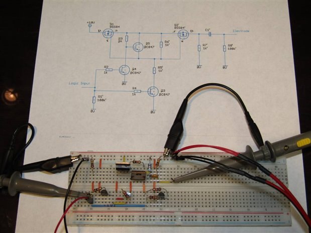
    The circuit that you posted for Von looked very interesting to me and so I did a facsimile bread board of it and ran signal and looked at the output with the scope. I say facsimile as I used two IRF9520s for the P Ch FETS as this is what I had convenient and I used 2N222 NPN general purpose transistors to substitute for your SMD transistors. Here is what it looked like:


    image

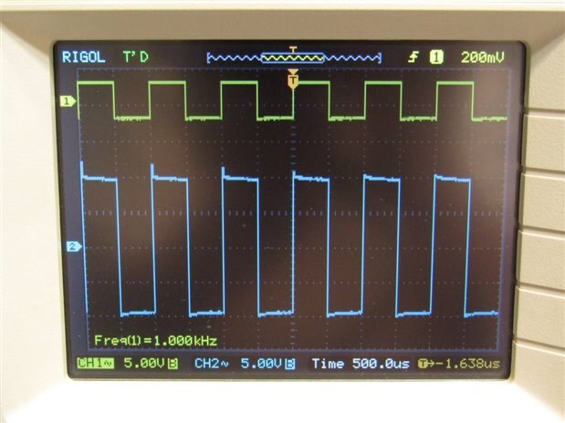
    Channel 1 Yellow is input and channel 2 Blue is the output. I ran a Square 1 kHz 5 volts PP signal into the input and this is what I got on the unloaded output:


    image


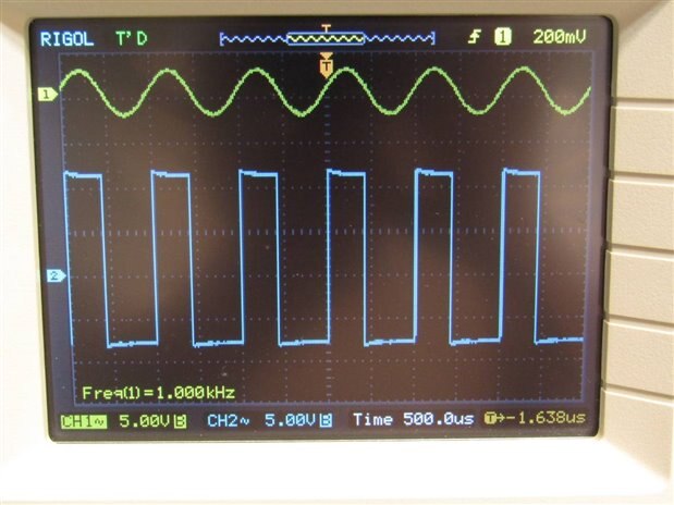
    The Vdd was set at 19 volts and you can see that the circuit performed just as you indicated it would. I switched over to a sine wave input and the output continued as a quite nice clean square wave.


    image


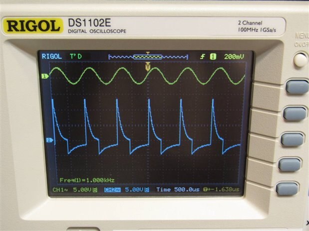
    Finally I decided to load the output. Some preliminary tests have indicated that real world loads may be in the range of 200 to 400 ohms so I used a 330R resistor and as would be expected the loading of the circuit through the capacitor modified the output signal to this:


    image


    Von is coming over at 2:30 tomorrow PM and I have left the circuit set up on the bench in case he wants to run any experiments on it. Thanks for your help and the fun I had tonight playing with this circuit.


    John

    • Cancel
    • Vote Up +6 Vote Down
    • Sign in to reply
    • Cancel
  • vwolff
    vwolff over 8 years ago in reply to genebren

    Thanks Gene.  That is very interesting.

    • Cancel
    • Vote Up +1 Vote Down
    • Sign in to reply
    • Cancel
  • vwolff
    vwolff over 8 years ago in reply to shabaz

    Thanks shabaz.  That is very interesting.

    • Cancel
    • Vote Up +2 Vote Down
    • Sign in to reply
    • Cancel
  • shabaz
    shabaz over 8 years ago in reply to vwolff

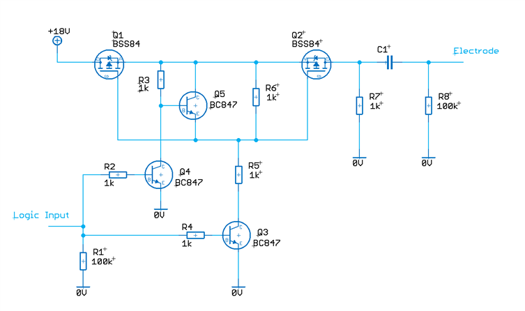
    Hi Von,


    Here is my attempt, it took a few more transistors that I anticipated once I examined the document a bit more. It uses a similar scheme to genebren, in fact you can reduce the design components by swapping out Q2 and Q3 to become the parts on the right side of his diagram (I used a bipolar transistor for the lower one, but the design can become smaller by using a MOSFET in one half of a package instead).


    As for the rest of the circuit, Q1 is there to block reverse current when the electrode is off, in case the electrode sees power (i.e. from the other electrodes when they are energised). Q5 is used to accelerate the turning off of the two MOSFETs, because although the pulses are needed at a slow rate (5msec), the pulses are very narrow, down to less than 0.3usec according to the doc. So basically Q5 allows the gate voltage to quickly rise. Q4 drives it. R1 is there so that if the board is unplugged from the logic side circuitry, the electrode outputs are off by default.


    The circuit will have a peak of perhaps 50mA, but the pulses are very narrow and only one channel is on at a time, so hopefully this is acceptable, since the average current will be much lower (less than 1mA). R5 and R6 by the way also act as a potential divider when Q3 switches on, so that the gate isn't pulled as low as 0V (there is a bit of headroom anyway, since the small MOSFETs can have up to -20V for VGS max, and I think your design needs support up to 19V).


    Anyway this is just one possible approach, another could be to have a push/pull system rather than the design here. Also as mentioned the component count could be reduced by using Gene's dual MOSFET implementation for the output.

    The +18V is the desired voltage for the electrode, so if you want to have it adaptable, then maybe a small patch panel type area could be used, where (say) there are three supply voltages and any of them can be wired to a channel, with jumpers, e.g. those two pin jumpers that were popular on old PC motherboards.

    image

    • Cancel
    • Vote Up +5 Vote Down
    • Sign in to reply
    • Cancel
  • genebren
    genebren over 8 years ago in reply to vwolff

    Hi Von,


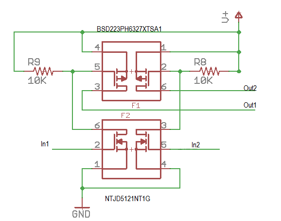
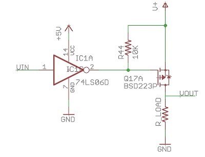
    I think that shabaz is on the money with a MOSFET solution that would provide greater currents, with little to no wasted power.  Attached is a circuit that I use in several different designs, that are High side drivers (2), built from a two dual MOSFET devices (1 N-channel and 1 P-channel).  The part are pretty inexpensive (BSD223 are $.22 in quantity of 100, and the NTJD512NT1G are $.18 in quantity of 100), yielding a driver cost of ~$0.20 per channel.


    image

    The inputs are driven by either 3.3V or 5.0V and the outputs are capable of driving 20V at ~390mA.  The outputs would need some load (not shown in this example, but >10K should work fine).

    I hope this helps.

    Gene

    • Cancel
    • Vote Up +5 Vote Down
    • Sign in to reply
    • Cancel
  • shabaz
    shabaz over 8 years ago in reply to vwolff

    Hi Von,


    Thanks for the info, it is clear now. I think your design will work, however the amount of current that can be sourced is low, because the 74LS06 pulls low, so the only control you have is through the pull-up resistors. You'd be able to source more current (and have it more efficient) by having high-side drivers, instead of low-side.

    The only problem with high-side is that there are not so many options in terms of ICs. An example IC is LMD18400, however it has only 4 channels and is expensive, and also has all four channel voltage source connected together, so it's not possible to set some channels to 19V, and some to (say) 17V and so on.

    Others could have solutions I may have missed, but I currently believe a discrete solution to replace the 'LS06 may be better, and it could be done with about three MOSFETs per channel, and some DIL patch panel type area for selecting what voltages you want to assign (out of say a few discrete setting like 19V, 18V and 17V) to each channel. It would be cheaper, and wouldn't be too large, because they don't need to be power MOSFETs. Surface mount could be used, e.g. SOT-23 sized which is easy to hand-solder.

    If you think that's the way to go, I can sketch out the topology for a channel (it would just be repeated for all channels) and it would then connect to your 'LS154.  'LS is quite ancient, you may find it easier to obtain HC or HCT parts. Owing to the number of channels, I think surface mount is definitely the way to go (John also has experience with SMD) and the larger SMD parts could be chosen to keep it very easy to assemble.

    Also if it is designed so there is separation after the '154, e.g. a separate PCB, using header pins to connect for instance, then at a later date you could swap out the controller board with a microcontroller, if (say) you wished to adapt the output pattern.

    • Cancel
    • Vote Up +4 Vote Down
    • Sign in to reply
    • Cancel
  • vwolff
    vwolff over 8 years ago in reply to shabaz

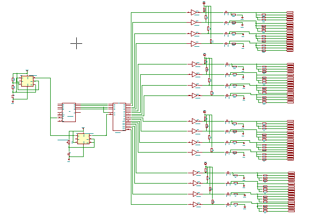
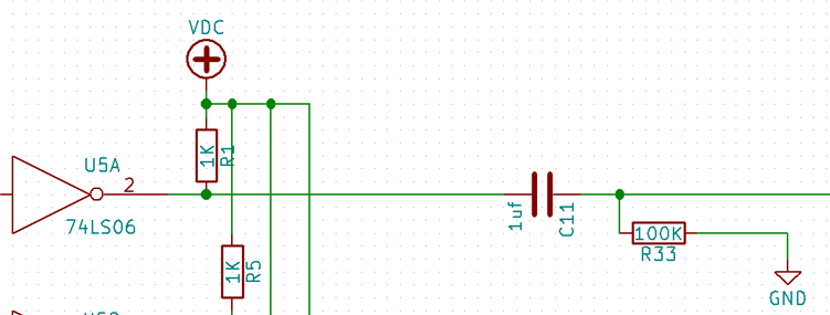
    The overall schematic:

    image


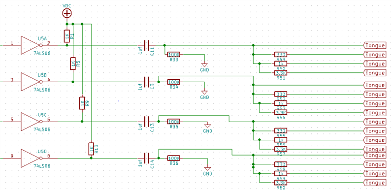
    Zooming in a bit:


    image

    and zooming in more:

    image


    The "VDC" is 19 volts.   I think the 1K pullup resistor could be a larger value and still supply enough current?  What do you think?


    Thanks,

    Von

    • Cancel
    • Vote Up +5 Vote Down
    • Sign in to reply
    • Cancel
  • shabaz
    shabaz over 8 years ago in reply to vwolff

    Hi Von,


    I didn't understand how you were using the 74LS06 to select the voltage level. If you have a sketch that would be awesome.

    In any case, if the output is from a logic gate with totem-pole type output stage, then the 1k resistors are not needed. Otherwise, they would be needed I think.

    • Cancel
    • Vote Up +1 Vote Down
    • Sign in to reply
    • Cancel
  • vwolff
    vwolff over 8 years ago in reply to shabaz

    I'm using logic gates:  A 74LS154 as a mux driving 74LS06 open collector inverters to Shift the voltage level. Thanks again

    • Cancel
    • Vote Up +2 Vote Down
    • Sign in to reply
    • Cancel
  • shabaz
    shabaz over 8 years ago in reply to vwolff

    Hi Von,


    Is your circuit using analogue multiplexers like in the diagram, or instead using logic gates? If the latter, then the 1k resistors are not needed, because the logic '0' state acts like the low impedance to ground anyway. I too was thinking (before I saw the diagrams) that the outputs could just have high and low driving MOSFETs or logic gates, to eliminate the need for the resistors and save a bit of power as you say.

    • Cancel
    • Vote Up +2 Vote Down
    • Sign in to reply
    • Cancel
Reply
  • shabaz
    shabaz over 8 years ago in reply to vwolff

    Hi Von,


    Is your circuit using analogue multiplexers like in the diagram, or instead using logic gates? If the latter, then the 1k resistors are not needed, because the logic '0' state acts like the low impedance to ground anyway. I too was thinking (before I saw the diagrams) that the outputs could just have high and low driving MOSFETs or logic gates, to eliminate the need for the resistors and save a bit of power as you say.

    • Cancel
    • Vote Up +2 Vote Down
    • Sign in to reply
    • Cancel
Children
  • genebren
    genebren over 8 years ago in reply to jw0752

    John,


    The signals look good.  I really like the way you were able to modularize the driver onto a single adapter.  Very cool!


    Gene

    • Cancel
    • Vote Up +3 Vote Down
    • Sign in to reply
    • Cancel
  • jw0752
    jw0752 over 8 years ago in reply to michaelkellett

    Hi Michael,

    I love electronics, there are so many elegant ways to get from point A to point B. there are even some inelegant ways as evidenced from some of my own designs. I will mention your idea to Von. We are probably locked into the present path though as the parts have been ordered and time is of the essence to Von. Thank you for the idea. I am always interested in what you have to say.

    John

    • Cancel
    • Vote Up +4 Vote Down
    • Sign in to reply
    • Cancel
  • michaelkellett
    michaelkellett over 8 years ago in reply to jw0752

    I've come very late to this discussion - only spotted it today.


    This may be a daft suggestion but here goes:


    Why not just use a quad op amp as the driver - may not be optimum for cost but an OPA4192 can do 0 - 30V, 20V/us slew rate, 10 mA drive easily, more for non continuous operation.


    Can get it in a TSSOP14 package so it's tiny. Resistors in 0402 or 4 in 1206 won't take up much space.


    Let me know if the idea is appealing and I'll think of a circuit.


    MK

    • Cancel
    • Vote Up +5 Vote Down
    • Sign in to reply
    • Cancel
  • jw0752
    jw0752 over 8 years ago in reply to genebren

    Hi Gene,

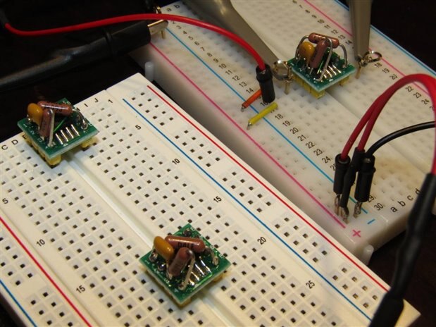
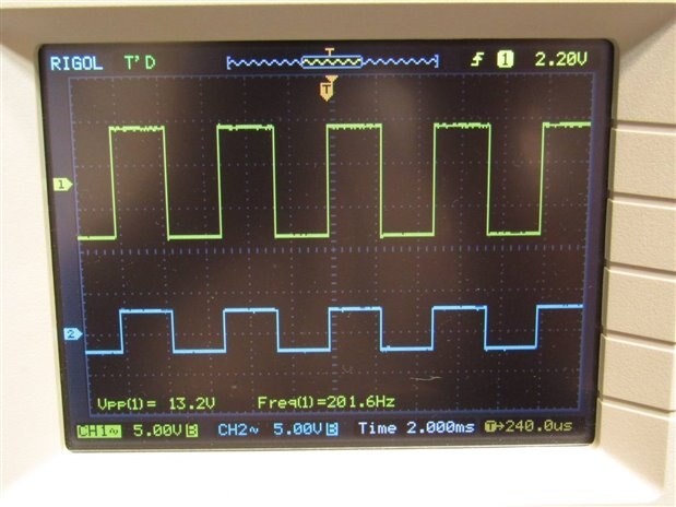
    Von and I spent a couple hours today testing the MOSFET circuit that you recommended. We are using a TC2320 chip which has one N Ch and one P Ch chip in an SOIC 8 package. This allows us to put one driver circuit on each bread board adapter. I was also able to pull the other peripheral passives up onto the little adapter board. We will be able to drive one each of Von's 16 channels with each module and all we will have for external connections are power rails and one input and one output. We both want to thank you for the good solution to increasing the output of the device.

    image


    image

    The blue is the signal from the generator and the yellow is the output from the MOSFET module.


    John

    • Cancel
    • Vote Up +2 Vote Down
    • Sign in to reply
    • Cancel
  • genebren
    genebren over 8 years ago in reply to jw0752

    John,


    The N-Channel MOSFET acts as an open drain inverter, so replacing it with an open collector inverter works fine.  Or, you could leave out the 7406 and drive an N-channel MOSFET directly (as shown in the initial reply).  Either way should work fine.


    Gene

    • Cancel
    • Vote Up +1 Vote Down
    • Sign in to reply
    • Cancel
  • jw0752
    jw0752 over 8 years ago in reply to genebren

    Is there any advantage to the two stages using the P Ch as a switch and the N Ch as a driver? I have some TC2320 chips which house one of each.


    John

    • Cancel
    • Vote Up +1 Vote Down
    • Sign in to reply
    • Cancel
  • genebren
    genebren over 8 years ago in reply to jw0752

    John,


    Here is a quick sketch of how you could do this with a 7406 (open collector) to switch the high-side MOSFET.  Shown is a single channel.

    image


    Gene

    • Cancel
    • Vote Up +2 Vote Down
    • Sign in to reply
    • Cancel
  • jw0752
    jw0752 over 8 years ago in reply to genebren

    Hi Gene,

    I am trying to set up a bread board of the circuit you proposed using the BSD 223.  If I am using the output of a 7406 for the input how do I interface. Do I have one channel or do I have two with the 2 inputs and 2 outputs. Von may understand but I don't and I am trying to set up the experiment before he comes in the next few days.


    John

    • Cancel
    • Vote Up +2 Vote Down
    • Sign in to reply
    • Cancel
  • fmilburn
    fmilburn over 8 years ago in reply to jw0752

    Great!

    • Cancel
    • Vote Up +3 Vote Down
    • Sign in to reply
    • Cancel
  • jw0752
    jw0752 over 8 years ago in reply to fmilburn

    Hi Frank,

    An extra thank you as Von and I were able to collaborate to fix the power supply in large part to having the schematics and parts list.

    John

    • Cancel
    • Vote Up +3 Vote Down
    • Sign in to reply
    • Cancel
element14 Community

element14 is the first online community specifically for engineers. Connect with your peers and get expert answers to your questions.

  • Members
  • Learn
  • Technologies
  • Challenges & Projects
  • Products
  • Store
  • About Us
  • Feedback & Support
  • FAQs
  • Terms of Use
  • Privacy Policy
  • Legal and Copyright Notices
  • Sitemap
  • Cookies

An Avnet Company © 2026 Premier Farnell Limited. All Rights Reserved.

Premier Farnell Ltd, registered in England and Wales (no 00876412), registered office: Farnell House, Forge Lane, Leeds LS12 2NE.

Follow element14

  • X
  • Facebook
  • linkedin
  • YouTube