


We know SPI as a 4*-wire protocol. But it doesn't have to be. I'm checking high speed SPI data transfer with buffers, DMA and parallel data lines.
This time, I'm preparing a test bed for SPI with Buffers and DMA. Some hardcore memory probing going on. |

Buffers and DMA
Before we look for hardware performance boosters, let's check what we can do on the firmware side.
A typical speed kicker is using buffers and direct memory access (DMA).
We all typically start of our SPI communication with a loop that sends values byte per byte (or word per word).
Many controllers can do better. I'm using a Hercules controller that supports both buffered SPI and DMA.
Buffered SPI means that you can tell the SPI peripheral where your data sits, and how big it is.
The SPI module will then independently (and often without taking up processor power) physically stream the data.
That's already a good thing. It decreases the amount of context switching between controller and SPI module by the number of data elements you manage to buffer.
The second option, DMA, adds another win.
Your SPI module doesn't even need the controller to get at the data in that case.
Even though the data won't be delivered to the destination at the time you post it, you can walk away and do other things.
Use case: Draw a Bitmap on an LCD
I'm going to try this out on a 128 x 128 colour LCD.
I have a naive implementation that sends pixel per pixel via SPI.
I'll try to boost performance first by using a line buffer.
The SPI module can then move this bitmap line as a single operation to the LCD.
The second exercise is to enable DMA, and have the SPI do the exchange all by itself.
In a last phase, I'll try to work with two buffers, and fill the data for line 2 while line 1 is being drawn.
Naive Implementation of the BitMap Draw
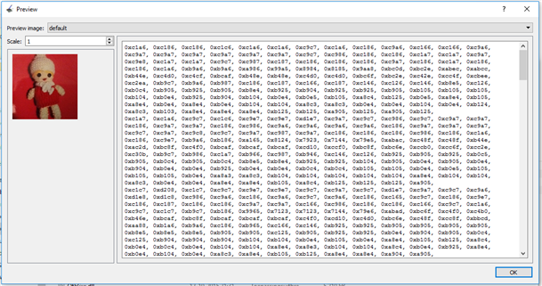
The image will be available in our code as a big array of pixels. The array contains 16-bit values. Each position just contains the RGB colour of that particular pixel. My LCD is 128*128. My array has 16384 positions.
I used Vladimir Rioson's LCD Image Converter - I'll have to spend another blog on the process to get the data in firmware |
I started off with the simplest draw function possible.
For each horizontal line, I iterate through all the pixels and draw them on the correct position.
    for (yy = 0; yy < bmp->height; yy++) {
        for (xx = 0; xx < bmp->width; xx++) {
            point(xx, yy, (bmp->data)[(yy)*bmp->height + (xx) ]);
        }
    }
Each time we call the point() function, we execute 8 SPI calls. That results in 16K * 8 = 131K SPI calls.
It's almost a miracle that it draws in less than a second.
(I'm using my own Hercules Educational BoosterPack MKII LCD library, ported from the Energia one for that display)
Preparation: Special Memory for MDA and Filling the Buffer Line
DMA needs some preparation. On the Hercules, the memory is by default configured to maximise caching.
It only writes info from cache to the real mem when it's needed by the core.
That's cool as long as it's only the ARM core that talks to that memory. But in our DMA set-up, that's not the case.
The SPI module will hit that memory in parallel with the core.
Any cashing scheme that doesn't immediately write through to the physical memory, fails. So we have to make special provisionings.
It would be stupid to make all memory write-through. That would impact the performance of our controller badly.
What we can do instead is to reserve a specific piece of RAM for the buffers, and make that shared.
We'll call this memory area SHAREDRAM. We'll steal this are from the normal configured RAM  .
.
I will create a buffer for one bitmap line. That's 128 colour values.
Because SPI exchanges data both ways during each clock tick, we'll also have to provide a receive button - even though our LCD display will never send data back.
One line is 128 values.
So we'll need one buffer of 128 positions for send data (that's 0x0100 in HEX for a 16-bit array - handy to know that for later). Automatically, we will need to provision a same sized receive buffer.
In total, we'll need the double to accommodate receive data too (although it 'll stay unused).
Here's a snippet of the memory map. This file is generated during the build process, but showing it now will prove that we're good (you can also see that I've reserved 0x1000 in stead of 2 x 0x0100 positions).
MEMORY CONFIGURATION
name origin length used unused attr fill
---------------------- -------- --------- -------- -------- ---- --------
...
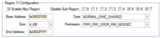
SHAREDRAM 0802f000 00001000 00000100 00000f00 RW
From Standard Memory Config to Dedicated DMA Area
When we create a Hercules project for the RM46 controller (the one I'm using here), all RAM is in one chunk.
RAM (RW) : origin=0x08001500 length=0x0002EB00
And all that RAM has the following attributes:
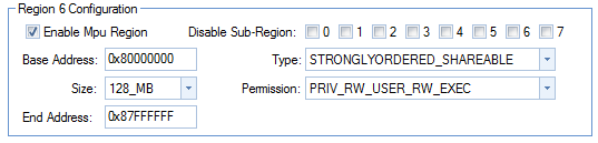
For our DMA, we'll need better than shareable. So we'll steal 256 positions from the RAM, and make it write-trough.
You'll need knowledge of your linker command file for that. I've blogged about that;
So we'll first nick room for those 256 positions from our RAM (I'm taking room for more here) , and call that chunk SHAREDRAM.
    RAM       (RW) : origin=0x08001500 length=0x0002DB00
    SHAREDRAM (RW) : origin=0x0802F000 length=0x00001000
(see how we decreased the RAM part by 0x01000?)
Let's now refine the cache properties of that little chunk, and make it write-trough.
Both ARM core and DMA will have the same view of the memory from now on. Guaranteed.
Getting our Buffers in Shared Memory
Now we'll have to place our buffers inside that SHAREDRAM.
We'll first add the directives for the linker in the linker command file.
.sharedRAM : {} > SHAREDRAM
That will instruct the linker to put all variables that are flagged as sharedRAM to go in our special shared memory location.
In our code, we use a #pragma to flag this special condition.
#pragma SET_DATA_SECTION(".sharedRAM")
uint16_t TXDATA[D_SIZE];         /* transmit buffer in sys ram */
uint16_t RXDATA[D_SIZE]= {0};    /* receive  buffer in sys ram */
#pragma SET_DATA_SECTION()
Everything after the first #pragma goes to the special area. Everything after the second #pragma to the default memory space for that type of source object.
Cool he? We've defined a special 4KB area with special cache handling. And we've managed to move our buffer into that area.
In the memory map file (created by the linker during the build, edited by me to only show the highlights), you'll find the proof.
MEMORY CONFIGURATION
         name            origin    length      used     unused   attr    fill
----------------------  --------  ---------  --------  --------  ----  --------
  RAM                   08001500   0002db00  0000a13c  000239c4  RW
  SHAREDRAM             0802f000   00001000  00000100  00000f00  RW

SEGMENT ALLOCATION MAP
run origin  load origin   length   init length attrs members
----------  ----------- ---------- ----------- ----- -------
0802f000    0802f000    00000100   00000000    rw-
  0802f000    0802f000    00000100   00000000    rw- .sharedRAM

SECTION ALLOCATION MAP
 output                                  attributes/
section   page    origin      length       input sections
--------  ----  ----------  ----------   ----------------
.sharedRAM
*          0    0802f000    00000100     UNINITIALIZED
                  0802f000    00000100     bitmaputils.obj (.sharedRAM:uninit)


GLOBAL SYMBOLS
address   name
-------   ----
0802f000  TXDATA
One thing that strikes out is: why is there only room allocated for the TXDATA buffer, and none for the RXDATA one?
That's because my code isn't finished, and I've not used the RXDATA buffer in my code yet. The linker kindly (and correctly) discards it.
Final Prep Step: Efficiently Filling the Buffer
Our code has to move a line of bitmap into the buffer efficiently. For us c aficionados, that means using memcpy().
We'll zap one line at a time from the full bitmap into the line array. Here's the code to do that.
memcpy(&TXDATA, (const void *)(bmp->data + (bmp->width) * row), 2 * D_SIZE);
Not much to be said here. We're copying a number of bytes (2 * D_SIZE) from the address of beginning of a row (bmp->data + (bmp->width) * row) to the buffer (&TXDATA).
Why 2 * D_SIZE? Because memcpy() copies a number of bytes. Our array exists of 16 bit values - and 16 bits is 2 bytes. it takes 2 times the array count to get all data moved.
What have we Achieved Now?
We have a buffer ready to optimise SPI traffic. The buffer is configured with the correct cache behaviour.
And we have a fast method to move bitmap chunks (lines) into that buffer.
We're all set up for the next stage, where we'll try to turn this into a fast SPI funnel.
Disclaimer: I haven't checked yet if my display actually accepts a series of values and paints them one after the other. We mai be in for a surprise if it doesn't.
Anyways, that doesn't impact the approach described here. I'll just not be able to show it for real then ...
Top Comments