element14 Community
element14 Community
    Register Log In
  • Site
  • Search
  • Log In Register
  • Community Hub
    Community Hub
    • What's New on element14
    • Feedback and Support
    • Benefits of Membership
    • Personal Blogs
    • Members Area
    • Achievement Levels
  • Learn
    Learn
    • Ask an Expert
    • eBooks
    • element14 presents
    • Learning Center
    • Tech Spotlight
    • STEM Academy
    • Webinars, Training and Events
    • Learning Groups
  • Technologies
    Technologies
    • 3D Printing
    • FPGA
    • Industrial Automation
    • Internet of Things
    • Power & Energy
    • Sensors
    • Technology Groups
  • Challenges & Projects
    Challenges & Projects
    • Design Challenges
    • element14 presents Projects
    • Project14
    • Arduino Projects
    • Raspberry Pi Projects
    • Project Groups
  • Products
    Products
    • Arduino
    • Avnet Boards Community
    • Dev Tools
    • Manufacturers
    • Multicomp Pro
    • Product Groups
    • Raspberry Pi
    • RoadTests & Reviews
  • Store
    Store
    • Visit Your Store
    • Choose another store...
      • Europe
      •  Austria (German)
      •  Belgium (Dutch, French)
      •  Bulgaria (Bulgarian)
      •  Czech Republic (Czech)
      •  Denmark (Danish)
      •  Estonia (Estonian)
      •  Finland (Finnish)
      •  France (French)
      •  Germany (German)
      •  Hungary (Hungarian)
      •  Ireland
      •  Israel
      •  Italy (Italian)
      •  Latvia (Latvian)
      •  
      •  Lithuania (Lithuanian)
      •  Netherlands (Dutch)
      •  Norway (Norwegian)
      •  Poland (Polish)
      •  Portugal (Portuguese)
      •  Romania (Romanian)
      •  Russia (Russian)
      •  Slovakia (Slovak)
      •  Slovenia (Slovenian)
      •  Spain (Spanish)
      •  Sweden (Swedish)
      •  Switzerland(German, French)
      •  Turkey (Turkish)
      •  United Kingdom
      • Asia Pacific
      •  Australia
      •  China
      •  Hong Kong
      •  India
      •  Korea (Korean)
      •  Malaysia
      •  New Zealand
      •  Philippines
      •  Singapore
      •  Taiwan
      •  Thailand (Thai)
      • Americas
      •  Brazil (Portuguese)
      •  Canada
      •  Mexico (Spanish)
      •  United States
      Can't find the country/region you're looking for? Visit our export site or find a local distributor.
  • Translate
  • Profile
  • Settings
Personal Blogs
  • Community Hub
  • More
Personal Blogs
Legacy Personal Blogs Thoughts on Scaling and Biasing an ADC Input Signal
  • Blog
  • Documents
  • Mentions
  • Sub-Groups
  • Tags
  • More
  • Cancel
  • New
  • Share
  • More
  • Cancel
Group Actions
  • Group RSS
  • More
  • Cancel
Engagement
  • Author Author: Andrew J
  • Date Created: 17 May 2020 5:45 PM Date Created
  • Views 4044 views
  • Likes 1 like
  • Comments 4 comments
Related
Recommended

Thoughts on Scaling and Biasing an ADC Input Signal

Andrew J
Andrew J
17 May 2020

I've been spending some time thinking about best using an ADC and I've done some weighing up of suitable components.  I've half settled on a Microchip MCP3248 rather than a TI ADS1115.  The Microchip has slightly better specs than the TI but it is limited in range on its inputs: -2.048V to +2.047V differential, 0V to +2.047V single ended; the TI has a more flexible option of ranges which expands its single-ended ranges, including a -4.096V to +4.096V, 0V to +4.096V single ended.


Anyway that's not really the purpose of this post per se except in so much that I may change my mind on the Microchip.  Currently, I would be limited to a 0V to 2.047V signal range which is half its available Full Scale Resolution (FSR); this is half that of the TI of course.  The range is fine if, for example, I had to sample a voltage drop over a current sense resistor but not so much if I had to measure a voltage of, say, 0V to 5V.  I'm describing here an option I'm considering to improve the resolution of the ADC and I thought it might make an interesting read.  I want to change an incoming 0V to 5V signal to a -2.048V to +2.048 signal to make full use of the ADCs FSR.


The datasheet has this to say:

The differential voltage at the input pins (without PGA) is:  Vin = CH+ - Ch-.  The differential input voltage range is -Vref <= Vin * PGA <= Vref - 1LSB; essentially the input range is -2.048V to +2.048V after applying any gain.

What this means is that I cannot apply a 0V-4.095V on the CH+ pin with a -2.048V on the CH-.  So if I scaled 5V to 4.095 on CH+ with -2.048V on CH- then Vin, according to the formula is 4.095 - (-2.048) = 6.143V.  I have to scale 0V to 5V to a range -2.048V to 2.047V and apply a -2.048V on the CH- pin.


In software, I could lift the output code up by 2.048V output code so -2.048 becomes 0V.


I'm working from this document which explains the maths and design very well.  I'm summarising a lot here, and missing out a fair bit of the algebraic manipulation so it's worth reading the document for a full understanding.  This is new to me, so here goes.


Scaling and biasing just means creating a new signal from an incoming signal as a linear transformation.  This can be represented by formula Vout = s * Vin + b, where s is the scale and b is the bias; the formula will look familiar to anyone who has graphed a straight line and it's essentially the same formula as the transfer function in a DAC and ADC - scale and bias are just synonyms for slope and offset.  Given two points on a straight line, we can calculate:

Scale = deltaVout / deltaVin

Bias = Vout - scale * Vin

With those two equations we can specify an input and output range and determine the scale and bias.


Easy Example

Map a 0V to 5V signal to a 0V to 2.048V signal.

  1. deltaVout is 2.048 and deltaVin is 5
  2. scale, s = 2.048 / 5 = 0.4096
  3. When Vout is 0 then Vin is 0 so Bias, b = Vout - s * Vin = 0 - 0.4096 * 0 = 0
  4. The final transformation for this is, Vout = 0.4096 * Vin + 0


Specific Calculation

Map a 0V to 5V signal to -2.048 to 2.047 signal

  1. deltaVout = 4.095, deltaVin = 5
  2. s = 4.095 / 5 = 0.819
  3. When Vout = 0 then Vin is 2.5 so b = 0 - 0.819 * 2.5 = -2.0475
  4. The final transformation for my need, then, is Vout = 0.819 * Vin + (-2.0475)


That's easy enough but this transformation has to be implemented through a voltage divider and a bias voltage source:


image

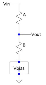
Vout can be calculated as, Vout = [B/(A+B)] * Vin + [A/(A+B)] * Vbias

Which looks just like the original linear transformation, Vout = s * Vin + b so

s =  [B/(A+B)]

b = [A/(A+B)] * Vbias

This work quite well in general terms.  Make A = B and choose 5V for Vbias and -5V to 5V maps into 0V to 5V.  Not what I need but shows the principle.


From all this, and doing the necessary algebraic finagling between these formulas we can calculate:

ratio of divider, r = deltaVout / (deltaVin - deltaVout) = 4.095 / (5 - 4.095) = 4.525

Vbias = Vout - r * (Vin - Vout) = 0 - 4.525 * (2.5 - 0) = -11.3125V [where Vout = 0 when Vin = 2.5]

LTSpice confirms this:

image


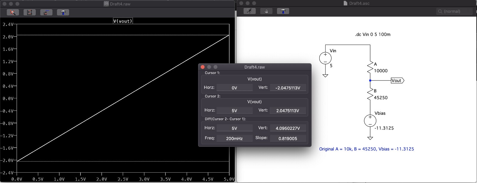
But -11.3125V isn't a very convenient value!  Turns out that I can make the Vbias part of the design and choose that value up front.


There's a lot of algebraic finagling and maths in this next step - add a third resistor.  I can't begin to explain it simply - it involves linearity and superposition of partial results - and just in case anyone thinks I'm a bit of a maths genius, let me burst that bubble and point you, again, at this document.  It explains better than I can what is going on here.


Nonetheless, I shall put some brief notes here.  In order to specify the Vbias voltage, we use three resistors as follows:

image


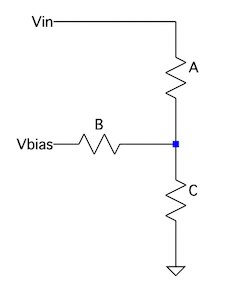
The basic formula from this is (gird your loins):

Vout = [ ((B * C) / (B + C)) / (A + ((B * C) / (B + C))) ] * Vin + [ ((A * C) / (A + C)) / (B + ((A * C) / (A + C))) ] * Vbias


It looks complicated but you can still see the scale and bias linear transformation in it.  From this we want to supply scale, bias and Vbias in order to calculate the values of resistors A, B and C.  There then follows a fair bit of algebra work (explained in the linked document) to end up with new looking (but the same) formulas for scale and bias:

s = ( 1 / [ A * (1/A + 1/B + 1/C) ] )

b = ( 1 / [ B * (1/A + 1/B + 1/C ] ) * Vbias

which is just a re-arrangement of the above complex formula in different algebraic terms.  Multiplying top and bottom of both by C:

s = ( (C/A) / (C/A + C/B + 1) )

b = ( (C/B ) / (C/A + C/B + 1) ) * Vbias

Here it gets tricky. We can work those formula through with a scaling factor alpha=(1/A + 1/B + 1/C) and end up with

s = 1 / Aalpha

b = Vbias / Balpha

and combining with the original formula for calculating s and b:

Aalpha = deltaVin / DeltaVout

Balpha = Vbias / (Vout - Vin / Aalpha)

Calpha = (Aalpha * Balpha) / (Aalpha * Balpha - Aalpha - Balpha)


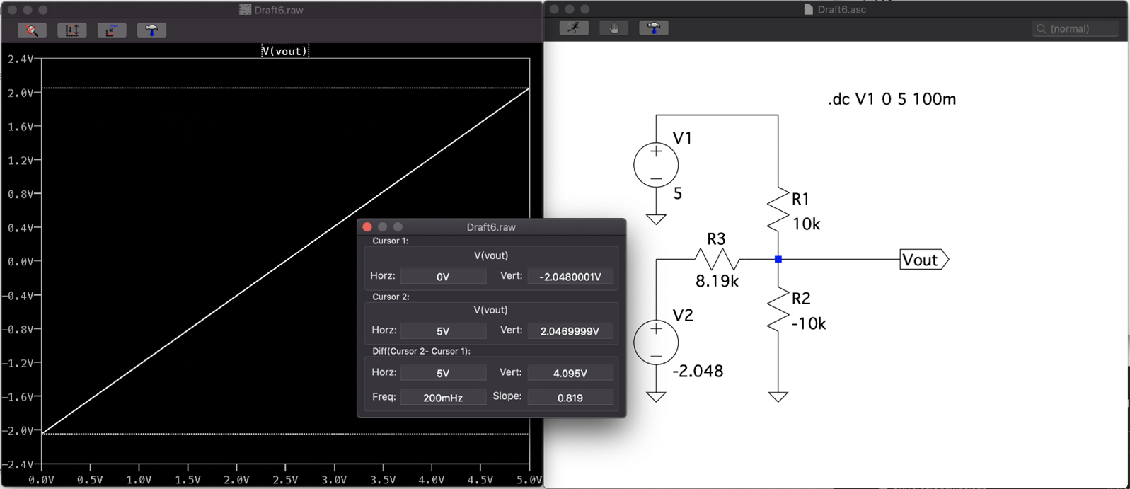
So, now we can work out the values for three resistor solution:

Vin = 0V to 5V, Vout = -2.048V to 2.047V, Vbias = -2.048V

Aalpha = 5 / 4.095 = 1.221

Balpha = -2.048 / (2.047 - 5 / 1.221) = 1 [when Vin is 5V, Vout is 2.047]

Calpha = (1.221 * 1) / (1.221 * 1 - 1.221 - 1) = -1.221 <------ Uh-oh!


A = (10K/1.221) * 1.221 = 10K

B = (10K/1.221) * 1 = 8.19K

C = (10K/1.221) * -1.221 = -10K   <------ !!


Clearly an unworkable solution except in LTSpice:

image


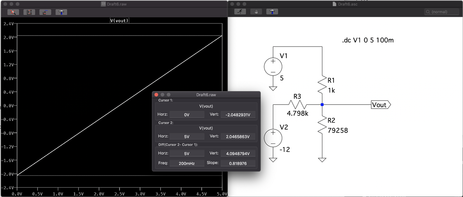
So there is only one option - change the output range and/or Vbias.  Keeping Vbias at -2.048 won't give any workable solutions and, in fact, the only workable solution I found was by changing Vbias from -2.048:

A -12Vbias would give me a full output range of -2.048V to 2.047V:

image

A -5Vbias would give me a range of 3.5V:

image

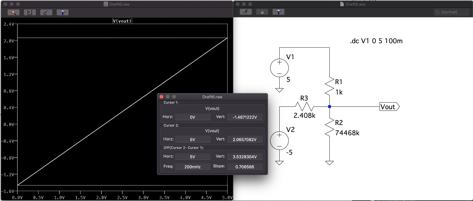
Note, changing the resistor values to obtainable values has a small impact on the range.


Either of these solutions still leaves me needing to create a -2.048V for the -ve differential input to the ADC.  If I did this, I would need the following power rails for the solution: +5V for the ICs, -5V for the buffering OpAmp, -12V for the bias voltage and -2.048V for the differential input.  Here's what it would look like in practice (including a not-calculated low pass filter before the ADC inputs):

image

Even in LTSpice without modelling any parasitics it's showing that it isn't perfect.  Of course, even without this, accuracy would still be impacted by parasitic and other circuit elements.  I wouldn't use an OPA192 to buffer the -2.048V in practice as it's too expensive so I'd just use a jelly bean part.


It's got me wondering if it's worth the effort and whether or not I should just stick to using the single ended range or switching to the ADS1115 with its larger single ended range.  For a different voltage range, e.g. 0 to 30V, a different set of values will be needed. 


Anyway, the main reason for posting this is I thought the whole process was interesting enough to share.

  • Sign in to reply

Top Comments

  • shabaz
    shabaz over 5 years ago +2
    Hi Andrew, I was going to say usually ADS1115 is an easy justification because it is low-cost, but it doesn't seem to be that any more, at least for one-offs. I don't understand TI pricing.. a circa £20…
  • shabaz
    shabaz over 5 years ago in reply to Andrew J +1
    Hi Andrew, The 0V to 5V would need to be converted into 0 to +2.048V, and +2.048V to 0V to make use of the full range of the differential input. Here's a mapping, assume 2 means 2.048V, note that VP and…
  • Andrew J
    Andrew J over 5 years ago in reply to shabaz +1
    Ah, I’ve completely misunderstood the datasheet haven’t I! Rather than the inputs taking 0 to +2.048 or 0 to -2.048 (giving a range of 4.096 if that full range was applied to the CH+ and CH-), each can…
Parents
  • shabaz
    shabaz over 5 years ago

    Hi Andrew,


    I was going to say usually ADS1115 is an easy justification because it is low-cost, but it doesn't seem to be that any more, at least for one-offs. I don't understand TI pricing.. a circa £20 dev-board for a different chip I was looking at is now over £200..

    There's no need for negative supplies or negative voltages to be buffered (or were you discussing the difference between two positive voltages?), the differential inputs can be driven from dual op-amps, known as a differential driver (example is ADA4941 but there are probably lower-cost alternatives, or it could be formed from two op amps). That will generate differential outputs centred around a value you choose based on an input reference voltage. For example, if your ADC only accepts 0-2.048V on its inputs, then you could use 1.024V as a reference. Then, your input, single-ended, between 0 and any positive voltage, will (theoretically) use the full range, based on the gain value you set (caveat; the op-amps won't completely go rail to rail, so you'll lose some range). By differential output I mean each of the two signals will be positive (i.e. between 0-2.048V for instance) but subtracting one from the other gets you the -2.048 to +2.048 range, and no negative supplies are used.

    However, if you just want to measure between 0V and 5V, it could be easier to just use a single ended ADC and if you definitely need the extra resolution you could choose (say) an 18-bit ADC, if all else is equal (which it rarely is!). I'm not sure I ever end up picking the 'right' ADC. But for 'just a redesign' for the input circuitry or references, something better or cheaper always seems to be missed : (

    • Cancel
    • Vote Up +2 Vote Down
    • Sign in to reply
    • More
    • Cancel
  • Andrew J
    Andrew J over 5 years ago in reply to shabaz

    Thanks Shabaz.  My basic idea was just to convert a 0V to 5V signal into -2.048v to 2.048 to make use of the available range of the ADC.  This isn’t really the way to go: these values work for 0 to 5V but different values are required for a different range. That’s fine when I’m just playing around and I thought it was interesting enough to post about.  I put buffer U1 in because the -ve voltage was sourced from a voltage divider which I thought would change depending on any resistive load on its output.

    I didn’t know such a thing as a differential driver existed but it seems like a more generalised solution to what I describe here.  I don’t fully follow what you say but I’ll check it out tomorrow and have a play with LTSpice. 


    There are precious few 16-bit I2C ADCs so choice is limited so I might give them both a go.

    • Cancel
    • Vote Up 0 Vote Down
    • Sign in to reply
    • More
    • Cancel
  • shabaz
    shabaz over 5 years ago in reply to Andrew J

    Hi Andrew,


    The 0V to 5V would need to be converted into 0 to +2.048V, and +2.048V to 0V to make use of the full range of the differential input.

    Here's a mapping, assume 2 means 2.048V, note that VP and VN columns are always positive numbers:


    DIFF   VP   VN
    -2     0    2
    -1     0.5  1.5
    0      1    1
    1      1.5  0.5
    2      2    0


    The 'differential' representation is just a mathematical term, it doesn't mean the the signal ever goes negative, i.e. the DIFF column is imaginary, and I could have written it as 0 to 4 instead of -2 to +2. VP minus VN represents that differential value.  So, you'd need to convert the 0 to 5V into two signals, one which goes high and the other which goes low, but both stay positive above 0V, i.e. the input must not have -2.048V on it, this is also in the electrical characteristics:

    image

    • Cancel
    • Vote Up +1 Vote Down
    • Sign in to reply
    • More
    • Cancel
  • Andrew J
    Andrew J over 5 years ago in reply to shabaz

    Ah, I’ve completely misunderstood the datasheet haven’t I!  Rather than the inputs taking 0 to +2.048 or 0 to -2.048 (giving a range of 4.096 if that full range was applied to the CH+ and CH-), each can have 0 to 2.048.  On that basis, with this ADC I absolutely might as well stick with using a single-ended input, and this is where the ADS1115 has an advantage as it can have different ranges - although that changes the LSB so doesn’t increase resolution it does allow more flexibility at the inputs.


    On the plus side, I did find working out that scaling and biasing fascinating - it wasn’t something I was aware of (well, voltage dividers I was of course.)


    I don’t know why the LTSpice images came out so big, they weren’t when I was creating the post.

    • Cancel
    • Vote Up +1 Vote Down
    • Sign in to reply
    • More
    • Cancel
Comment
  • Andrew J
    Andrew J over 5 years ago in reply to shabaz

    Ah, I’ve completely misunderstood the datasheet haven’t I!  Rather than the inputs taking 0 to +2.048 or 0 to -2.048 (giving a range of 4.096 if that full range was applied to the CH+ and CH-), each can have 0 to 2.048.  On that basis, with this ADC I absolutely might as well stick with using a single-ended input, and this is where the ADS1115 has an advantage as it can have different ranges - although that changes the LSB so doesn’t increase resolution it does allow more flexibility at the inputs.


    On the plus side, I did find working out that scaling and biasing fascinating - it wasn’t something I was aware of (well, voltage dividers I was of course.)


    I don’t know why the LTSpice images came out so big, they weren’t when I was creating the post.

    • Cancel
    • Vote Up +1 Vote Down
    • Sign in to reply
    • More
    • Cancel
Children
No Data
element14 Community

element14 is the first online community specifically for engineers. Connect with your peers and get expert answers to your questions.

  • Members
  • Learn
  • Technologies
  • Challenges & Projects
  • Products
  • Store
  • About Us
  • Feedback & Support
  • FAQs
  • Terms of Use
  • Privacy Policy
  • Legal and Copyright Notices
  • Sitemap
  • Cookies

An Avnet Company © 2025 Premier Farnell Limited. All Rights Reserved.

Premier Farnell Ltd, registered in England and Wales (no 00876412), registered office: Farnell House, Forge Lane, Leeds LS12 2NE.

ICP 备案号 10220084.

Follow element14

  • X
  • Facebook
  • linkedin
  • YouTube