element14 Community
element14 Community
    Register Log In
  • Site
  • Search
  • Log In Register
  • Members
    Members
    • Achievement Levels
    • Benefits of Membership
    • Feedback and Support
    • Members Area
    • Personal Blogs
    • What's New on element14
  • Learn
    Learn
    • eBooks
    • Learning Center
    • Learning Groups
    • STEM Academy
    • Webinars, Training and Events
  • Technologies
    Technologies
    • 3D Printing
    • Experts & Guidance
    • FPGA
    • Industrial Automation
    • Internet of Things
    • Power & Energy
    • Sensors
    • Technology Groups
  • Challenges & Projects
    Challenges & Projects
    • Arduino Projects
    • Design Challenges
    • element14 presents
    • Project14
    • Project Groups
    • Raspberry Pi Projects
  • Products
    Products
    • Arduino
    • Avnet Boards Community
    • Dev Tools
    • Manufacturers
    • Product Groups
    • Raspberry Pi
    • RoadTests & Reviews
  • Store
    Store
    • Visit Your Store
    • Or choose another store...
      • Europe
      •  Austria (German)
      •  Belgium (Dutch, French)
      •  Bulgaria (Bulgarian)
      •  Czech Republic (Czech)
      •  Denmark (Danish)
      •  Estonia (Estonian)
      •  Finland (Finnish)
      •  France (French)
      •  Germany (German)
      •  Hungary (Hungarian)
      •  Ireland
      •  Israel
      •  Italy (Italian)
      •  Latvia (Latvian)
      •  
      •  Lithuania (Lithuanian)
      •  Netherlands (Dutch)
      •  Norway (Norwegian)
      •  Poland (Polish)
      •  Portugal (Portuguese)
      •  Romania (Romanian)
      •  Russia (Russian)
      •  Slovakia (Slovak)
      •  Slovenia (Slovenian)
      •  Spain (Spanish)
      •  Sweden (Swedish)
      •  Switzerland(German, French)
      •  Turkey (Turkish)
      •  United Kingdom
      • Asia Pacific
      •  Australia
      •  China
      •  Hong Kong
      •  India
      •  Korea (Korean)
      •  Malaysia
      •  New Zealand
      •  Philippines
      •  Singapore
      •  Taiwan
      •  Thailand (Thai)
      • Americas
      •  Brazil (Portuguese)
      •  Canada
      •  Mexico (Spanish)
      •  United States
      Can't find the country/region you're looking for? Visit our export site or find a local distributor.
  • Translate
  • Profile
Personal Blogs
  • Members
  • More
Personal Blogs
Legacy Personal Blogs YAPS Part Five - Design - PCB
  • Blog
  • Documents
  • Mentions
  • Sub-Groups
  • Tags
  • More
  • Cancel
  • New
Blog Post Actions
  • Subscribe by email
  • More
  • Cancel
  • Share
  • Subscribe by email
  • More
  • Cancel
Group Actions
  • Group RSS
  • More
  • Cancel
Engagement
  • Author Author: Andrew J
  • Date Created: 29 May 2019 4:41 PM Date Created
  • Views 527 views
  • Likes 6 likes
  • Comments 8 comments
  • bench power supply
  • modular_bench_powersupply
Related
Recommended

YAPS Part Five - Design - PCB

Andrew J
Andrew J
29 May 2019

The KiCad files are available on Github.

Custom footprints and custom symbols can be downloaded from Github.  You’ll need to add a link to these in KiCad’s preferences so that the projects don’t error when opening.  I’m assuming that if you have KiCad you know how to do that, but please ask below.


There are two projects, one for the Power Stage and one for the Control Stage (actually called Power Supply.)


I have produced precisely zero PCB designs before - I don’t count the trial one I did of my first power supply I mentioned in Part One which was faintly praised with ‘It should work electrically” image  This is somewhat more complicated and I've added images below.


I set my own constraints when doing this:

  • follow layout guidance given in data sheets
  • use SMD parts, mostly, to keep the size down.  The exceptions were for parts that I don't own the proper tools to solder.
  • fit within 100mm x 100mm dimensions AND 2 layers to keep production costs down.  JLCPCB will create these at around £1.50 for 5 but the price jumps to £22 for a 4-layer board.
  • allow for 2mm between parts to let me to get a soldering iron in and (hopefully not) a hot-air nozzle if I have to rework it.  I really don’t want to buy one of those yet.
  • not split a ground plane by minimising bottom layer routing
  • take account of current capacity with track widths.


A note on the last point re track widths.  The ‘high current’ path is set at 1.5mm - this is greater than the minimum width calculated according to IPC-2221 for a 10 degree C temperature rise and well over the width required for a 20 C rise which I believe it could easily cope with.  It’s less than the minimum width calculated according to IPC-2152 for a 10 C rise but well over the width for a 20 C rise.  In either case, I couldn’t derive a width by specifying a voltage drop: the calculators didn’t allow it and I’m not sure what an acceptable drop would be as output isn't fixed.  It’s obviously not in line with a rule-of-thumb 1mm per Amp.  Ultimately, I traded off space and size against the real likelihood of extended running at 3A which is unlikely for me: for most operation it will be fine and I expect it will be ok at 3A as well.  Even at a 3A output, there isn't 3A flowing through all the high-current circuit (the LT3081s max at 1.5A for example.)  All other signal paths are well over-sized at 0.5mm or 0.35mm for what is small number of milliamps.


I’m also aware that I could have positioned the 5V supply better as its output is daisy-chained (mostly) to the parts that need it.  I didn’t bother to change it (I’d have to re-do the whole board) as the thermistors are single point routed so should get even voltage;  the INA260 can operate from 2.7 to 5.5V so will be sufficiently supplied.  Additionally, I could have laid out the resistors and capacitors aligned in one direction but again I traded off routing as little as possible on the bottom layer.


I had to create custom footprints and symbols but KiCad makes this reasonably easy to do.  It took a long time for me to complete this part, as I was taking my time, and I think that now I have a ‘worked example’, so to speak, I could probably do a bit better.  But actually, I don’t think it’s likely to suffer that much: more likely are other problems that require rework and which may require a new PCB - at that time, I’ll make some changes.
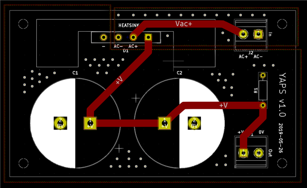
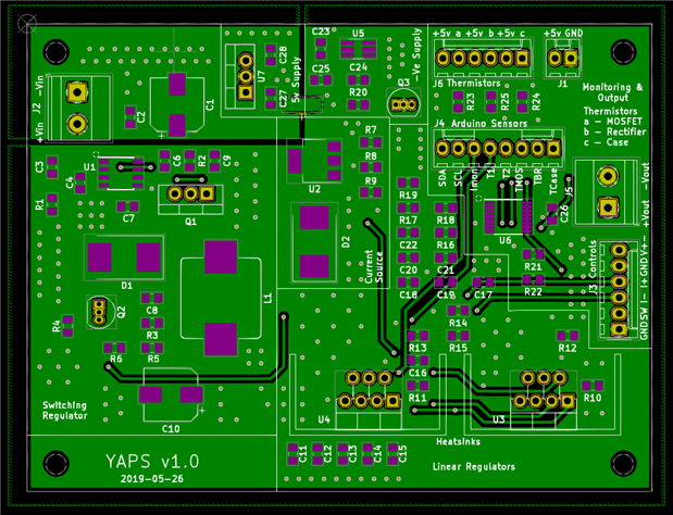
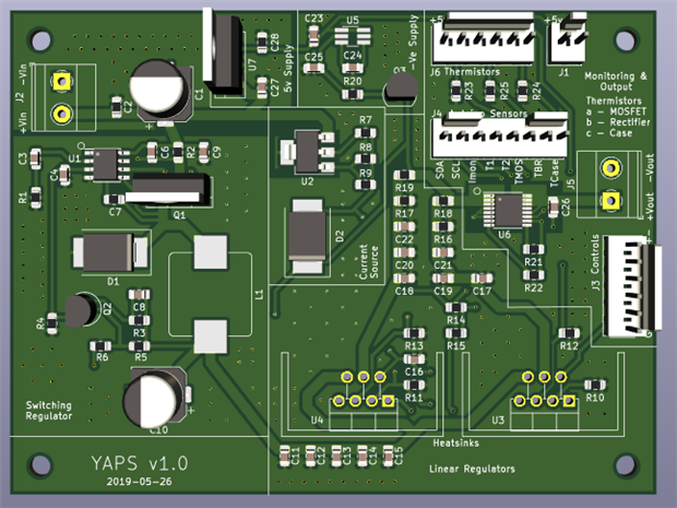
 

Power Stage PCB

Here's the component positioning and trace routing:

image

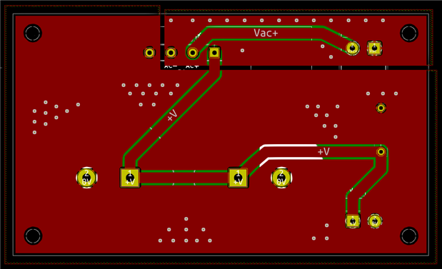
Front and Back planes for ground:

image

image

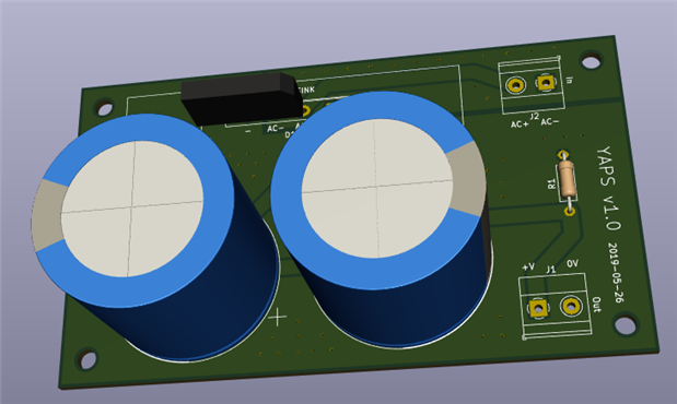
And a 3D view of front.  KiCad doesn't have 3D views for all parts so the terminal blocks aren't showing.  Also, note the bug in positioning of the rectifier:
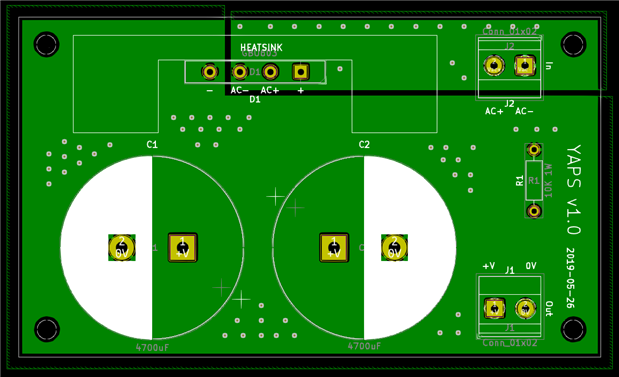
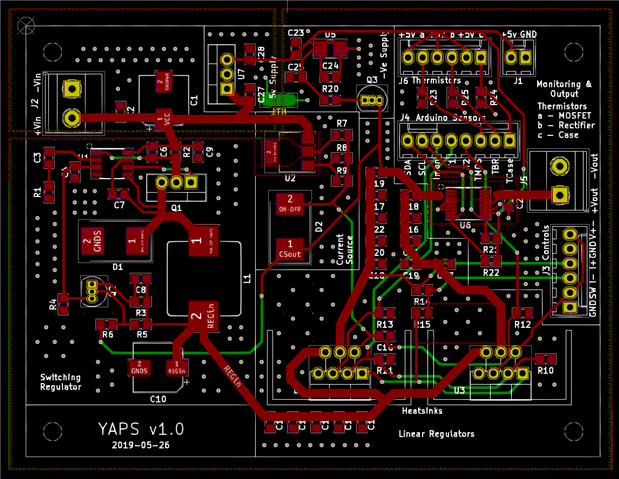
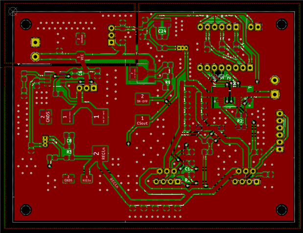
image


Control Stage PCB

Component positioning and trace routing:

image

Front and Back ground planes - joined with a net tie:

image

image

And a 3D view of the front.  Again, not all parts have a 3D view:

image


Next: Part Six - Design - BOM

Back: Part Four - Design - Calculations

  • Sign in to reply

Top Comments

  • Andrew J
    Andrew J over 4 years ago +1
    Always check the Gerbers! I found a few vias that were a little too close to the traces and intruded - not shown in PCBNew but clear as day in the Gerber. 5 each of the Power Stage and Power Control costs…
  • Andrew J
    Andrew J over 4 years ago +1
    PCBs arrived - took 6 days from placing the order to delivery in my hand. Look pretty good too.
  • shabaz
    shabaz over 4 years ago in reply to Andrew J +1
    Hi Andrew, This looks nice! I'd missed seeing this project earlier, but it looks like a lot of thought has gone into it. Looking forward to seeing the boards assembled.
Parents
  • Andrew J
    Andrew J over 4 years ago

    Bad news!  I found 3 problems on the Control Stage PCB all of my making.  I'd ordered a NPN in wide TO-92 rather than standard; The LT3081s come pre-bent - 3 legs back,  4 legs forward and I'd got it the other way around on the board; And I ordered the wrong package for the current source - a TSSOP rather than SOT-223.  All my fault, not taking enough care with ordering or reading the datasheet: I spent ages reading them as well, how I missed it I don't know.  I can only put it down to the picture at the front of the datasheet showing flat legs and I assumed I would bend them to fit.


    I can't fix these problems with a drill!  So I've updated the boards and re-ordered them so there will be a delay in progress.  Whilst I'm waiting I might as well work on the 4Duino interface.  I've not updated the images above as the updates don't change things significantly.


    Another lesson learned.

    • Cancel
    • Vote Up +1 Vote Down
    • Sign in to reply
    • More
    • Cancel
  • shabaz
    shabaz over 4 years ago in reply to Andrew J

    Hi Andrew,


    Sorry, I'm just reading this, and also saw that you're waiting on new boards. I still think you did an amazing job with the PCBs, and the entire project so far. Regarding the diode legs, I've hit that problem in the past too, small holes for diodes : ( so with EAGLE (I've not used KiCAD) I'll only rely on the 0603/0805 etc footprints, and self-create anything else (which means I've now got hundreds of custom parts created over the years).


    One thing that's missing on this site (I've seen some elsewhere, but I think it's possible to do a better job documenting here, so I hope someone creates it one day) is suggested steps or workflows before submitting PCB designs. It's something useful for all, since it can be easy for anyone to miss a step, and also a way to be quickly reminded that some assumptions might need to be checked. It would be nice to see a generic list (generally CAD system and PCB manufacturer agnostic so it's readable by all, but with brief software tips where it doesn't distract from readability). I've noticed I make lots of PCB mistakes when I'm tired, so for me I try to only submit a PCB design after a further 24 hours (with hopefully a few hours of thought in there : ) but a list of steps could help improve confidence a lot. Also it could suggest different coverage ideas, e.g. some things can be picked up by sharing PCB designs with others on the site for an informal review, and some things can be picked up by deliberately using a different gerber file viewer than the one built-in to the PCB design package, and so on.

    • Cancel
    • Vote Up +1 Vote Down
    • Sign in to reply
    • More
    • Cancel
Comment
  • shabaz
    shabaz over 4 years ago in reply to Andrew J

    Hi Andrew,


    Sorry, I'm just reading this, and also saw that you're waiting on new boards. I still think you did an amazing job with the PCBs, and the entire project so far. Regarding the diode legs, I've hit that problem in the past too, small holes for diodes : ( so with EAGLE (I've not used KiCAD) I'll only rely on the 0603/0805 etc footprints, and self-create anything else (which means I've now got hundreds of custom parts created over the years).


    One thing that's missing on this site (I've seen some elsewhere, but I think it's possible to do a better job documenting here, so I hope someone creates it one day) is suggested steps or workflows before submitting PCB designs. It's something useful for all, since it can be easy for anyone to miss a step, and also a way to be quickly reminded that some assumptions might need to be checked. It would be nice to see a generic list (generally CAD system and PCB manufacturer agnostic so it's readable by all, but with brief software tips where it doesn't distract from readability). I've noticed I make lots of PCB mistakes when I'm tired, so for me I try to only submit a PCB design after a further 24 hours (with hopefully a few hours of thought in there : ) but a list of steps could help improve confidence a lot. Also it could suggest different coverage ideas, e.g. some things can be picked up by sharing PCB designs with others on the site for an informal review, and some things can be picked up by deliberately using a different gerber file viewer than the one built-in to the PCB design package, and so on.

    • Cancel
    • Vote Up +1 Vote Down
    • Sign in to reply
    • More
    • Cancel
Children
  • Andrew J
    Andrew J over 4 years ago in reply to shabaz

    Hi Shabaz,


    That’s a great idea and I had planned to do a wrap up posting when I finish: I will make one specific to PCB that everyone can contribute to.


    I had ‘finished’ the PCB on the Wednesday I posted this entry but waited until the Sunday before ordering - I was hoping someone might take a look and point out problems, but in any case, I don’t think anyone else would/could have spotted these. 


    Like you, I’ve started building up a library of footprints based on components I’ve used here.  It’s small right now, but I’ve learnt my lesson here!

    • Cancel
    • Vote Up 0 Vote Down
    • Sign in to reply
    • More
    • Cancel
element14 Community

element14 is the first online community specifically for engineers. Connect with your peers and get expert answers to your questions.

  • Members
  • Learn
  • Technologies
  • Challenges & Projects
  • Products
  • Store
  • About Us
  • Feedback & Support
  • FAQs
  • Terms of Use
  • Privacy Policy
  • Legal and Copyright Notices
  • Sitemap
  • Cookies

An Avnet Company © 2023 Premier Farnell Limited. All Rights Reserved.

Premier Farnell Ltd, registered in England and Wales (no 00876412), registered office: Farnell House, Forge Lane, Leeds LS12 2NE.

ICP 备案号 10220084.

Follow element14

  • X
  • Facebook
  • linkedin
  • YouTube