element14 Community
element14 Community
    Register Log In
  • Site
  • Search
  • Log In Register
  • About Us
  • Community Hub
    Community Hub
    • What's New on element14
    • Feedback and Support
    • Benefits of Membership
    • Personal Blogs
    • Members Area
    • Achievement Levels
  • Learn
    Learn
    • Ask an Expert
    • eBooks
    • element14 presents
    • Learning Center
    • Tech Spotlight
    • STEM Academy
    • Webinars, Training and Events
    • Learning Groups
  • Technologies
    Technologies
    • 3D Printing
    • FPGA
    • Industrial Automation
    • Internet of Things
    • Power & Energy
    • Sensors
    • Technology Groups
  • Challenges & Projects
    Challenges & Projects
    • Design Challenges
    • element14 presents Projects
    • Project14
    • Arduino Projects
    • Raspberry Pi Projects
    • Project Groups
  • Products
    Products
    • Arduino
    • Avnet Boards Community
    • Dev Tools
    • Manufacturers
    • Multicomp Pro
    • Product Groups
    • Raspberry Pi
    • RoadTests & Reviews
  • Store
    Store
    • Visit Your Store
    • Choose another store...
      • Europe
      •  Austria (German)
      •  Belgium (Dutch, French)
      •  Bulgaria (Bulgarian)
      •  Czech Republic (Czech)
      •  Denmark (Danish)
      •  Estonia (Estonian)
      •  Finland (Finnish)
      •  France (French)
      •  Germany (German)
      •  Hungary (Hungarian)
      •  Ireland
      •  Israel
      •  Italy (Italian)
      •  Latvia (Latvian)
      •  
      •  Lithuania (Lithuanian)
      •  Netherlands (Dutch)
      •  Norway (Norwegian)
      •  Poland (Polish)
      •  Portugal (Portuguese)
      •  Romania (Romanian)
      •  Russia (Russian)
      •  Slovakia (Slovak)
      •  Slovenia (Slovenian)
      •  Spain (Spanish)
      •  Sweden (Swedish)
      •  Switzerland(German, French)
      •  Turkey (Turkish)
      •  United Kingdom
      • Asia Pacific
      •  Australia
      •  China
      •  Hong Kong
      •  India
      •  Korea (Korean)
      •  Malaysia
      •  New Zealand
      •  Philippines
      •  Singapore
      •  Taiwan
      •  Thailand (Thai)
      • Americas
      •  Brazil (Portuguese)
      •  Canada
      •  Mexico (Spanish)
      •  United States
      Can't find the country/region you're looking for? Visit our export site or find a local distributor.
  • Translate
  • Profile
  • Settings
Personal Blogs
  • Community Hub
  • More
Personal Blogs
Douglas Wong's Blog Who remembers EPROM?
  • Blog
  • Documents
  • Mentions
  • Sub-Groups
  • Tags
  • More
  • Cancel
  • New
  • Share
  • More
  • Cancel
Group Actions
  • Group RSS
  • More
  • Cancel
Engagement
  • Author Author: dougw
  • Date Created: 21 Oct 2021 5:34 AM Date Created
  • Views 5110 views
  • Likes 1 like
  • Comments 12 comments
  • doug wong
  • eprom
  • zynq mpsoc
  • raspberry pi hq camera microscope
  • 27512
Related
Recommended

Who remembers EPROM?

dougw
dougw
21 Oct 2021

This is just an off the wall way to say thank you to element14 and Xilinx. They had a little give-away draw to win a Zynq book and they ended up sending me a huge book called Exploring Zynq MPSoC and a screw driver set. I also recently completed a Project14 so I threw in some images from that project.

This is a digital microscope image of a 27512 EPROM. It took a lot of digging in my archives to find this chip, but I wanted a chip with a ready-made window so the microscope could image the actual silicon.

image

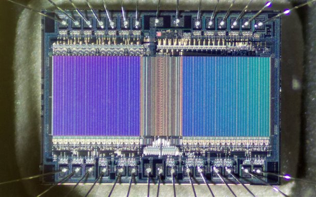
Click on the image for a full size view.

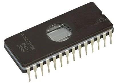
Here is what a typical EPROM looks like with its window to allow UV light to erase the memory:

image

I also took a a closer image just to see what this microscope can do....

image

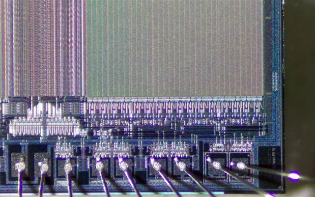
I'm having a lot of fun with this microscope.


Here is a video of the FPGA Technology Quiz prizes and the Pi HQ Camera microscope in action....

You don't have permission to edit metadata of this video.
Edit media
x
image
Upload Preview
image


I once used EPROM without a CPU as a look up table to convert 18 bit gray code to binary.

Have you ever tried to use sunlight to erase an EPROM?

Feel free to add your EPROM stories below, I'm sure there are lots of them.


Relevant Links:

FPGA Technology Quiz

I Spy With My Digital Eye .... a Pico PI

  • Sign in to reply
Parents
  • ralphjy
    ralphjy over 3 years ago

    We used UV eraseable eproms to store configuration data for the computer peripherals that we designed.


    I found my old UV eraser in with a bunch of old computer stuff.

    image


    I also found a sample box of ST parts circa late 80s.

    imageimage


    These were byte wide, so 4kx8 and 32kx8.  I must have used the 1 Meg eprom somewhere image.

    image

    • Cancel
    • Vote Up 0 Vote Down
    • Sign in to reply
    • More
    • Cancel
  • DAB
    DAB over 3 years ago in reply to ralphjy

    I still have one, I repurposed it to make UV light photographs.


    DAB

    • Cancel
    • Vote Up 0 Vote Down
    • Sign in to reply
    • More
    • Cancel
  • dougw
    dougw over 3 years ago in reply to DAB

    I always wanted a UV light to erase EPROMs, at least until EPROMs stopped being used.

    I wonder if UV light would erase EEPROM (or FLASH which is a type of EEPROM)

    • Cancel
    • Vote Up 0 Vote Down
    • Sign in to reply
    • More
    • Cancel
  • jc2048
    jc2048 over 3 years ago in reply to dougw

    My guess would be that the metallization on the surface is too dense with a Flash part (presumably the UV parts were deliberately designed with a clear area above much of the storage well for the light to get in), but I could be wrong.


    BTW thanks for the pictures. The one that shows clearly the welds of the bond wires is particularly nice. You can see, from the variation in the placement of the tack point, why they needed the landing pads the size they were.

    • Cancel
    • Vote Up 0 Vote Down
    • Sign in to reply
    • More
    • Cancel
  • jc2048
    jc2048 over 3 years ago in reply to dougw

    This is an explanation of the gate from the 1975 Intel Memory Design Handbook. This applies to the early parts like the 1702 and the 2704.


    image


    I was wrong to talk of a 'well' as it's really a floating gate formed above the substate within a grown insulating oxide layer, not sunk into it. Charge gets onto the gate by avalanching, so it's different to a Flash memory where the mechanism is tunneling. The diagram shows that the space above the gate is kept clear of metal to allow UV light to get to the charge on the floating gate.

    • Cancel
    • Vote Up 0 Vote Down
    • Sign in to reply
    • More
    • Cancel
Comment
  • jc2048
    jc2048 over 3 years ago in reply to dougw

    This is an explanation of the gate from the 1975 Intel Memory Design Handbook. This applies to the early parts like the 1702 and the 2704.


    image


    I was wrong to talk of a 'well' as it's really a floating gate formed above the substate within a grown insulating oxide layer, not sunk into it. Charge gets onto the gate by avalanching, so it's different to a Flash memory where the mechanism is tunneling. The diagram shows that the space above the gate is kept clear of metal to allow UV light to get to the charge on the floating gate.

    • Cancel
    • Vote Up 0 Vote Down
    • Sign in to reply
    • More
    • Cancel
Children
No Data
element14 Community

element14 is the first online community specifically for engineers. Connect with your peers and get expert answers to your questions.

  • Members
  • Learn
  • Technologies
  • Challenges & Projects
  • Products
  • Store
  • About Us
  • Feedback & Support
  • FAQs
  • Terms of Use
  • Privacy Policy
  • Legal and Copyright Notices
  • Sitemap
  • Cookies

An Avnet Company © 2025 Premier Farnell Limited. All Rights Reserved.

Premier Farnell Ltd, registered in England and Wales (no 00876412), registered office: Farnell House, Forge Lane, Leeds LS12 2NE.

ICP 备案号 10220084.

Follow element14

  • X
  • Facebook
  • linkedin
  • YouTube