10 Feb 2020 Update: Schematic and Bill of Materials updated
In a previous post a method for transferring art work to PCBs was described. I've been holding off sending it in until a circuit could be designed to go on the board. In this post a completed board is presented and the issues encountered described.
Circuit
The circuit is yet another LM386 audio amplifier with a few twists. Some of the usual modifications have been made:
- Additional decoupling for the power supply
- Addition of bass boost (fixed resistor)
- Addition of gain control
- Bypass capacitor on pin 7
- Large output capacitor
For a bit of a change it will be made with SMD parts on a custom PCB (with artwork :-).
PCB Design and Layout
There are some issues to address when using artwork with a working circuit on the PCB. The artwork itself is a footrpint and the Design Rule Check (DRC) may not catch errors when when vias or or through hole parts penetrate into the footprint. Among the ways to address this are:
- Make a one layer board with the art on the back and don't penetrate the PCB
- Penetrate outside the PCB footprint - the PCB must be larger in area than the art
- Carefully penetrate only grounded areas for grounds in the artwork (may not look good)
- Carefully penetrate only bare areas for wires in the artwork (may not look good)
- Mask out of the art design for circuitry (may not look good but could be a feature)
Approach 1 only works if there are no through holes or vias. Approach 2 means the artwork will be reduced in size. Approaches 3 through 5 modify the artwork appearance and may or may not look good.
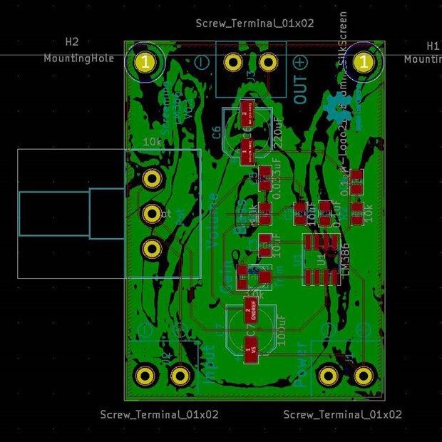
My approach turned out to be a combination of 1 and 5. Approach 2 would enlarge the board and increase cost or reduce an already small art design further. Approach 3 and 4 seemed to have risks for the first attempt at this and were discarded. The circuit itself is all on one layer but because screw terminals and mounting holes were desired for this design it was necessary to have penetrations. Accordingly, the art itselt was modified by masking out around all the holes in Photoshop. The new images were imported into KiCad and converted into a footprint as described in the previous blog. The footprint was then placed on the back of the PCB and the circuit drawn on the front layer.
| {gallery} Artwork with penetrations masked out |
|---|
Penetration Mask |
REPLACE THIS TEXT WITH YOUR IMAGE Copper Layer |
Mask Layer |
Silk Layer |
PCB Layout |
Renders of the design, front and back, are shown below. It looks like a Screaming LM386 doesn't it?
| {gallery} Renders of the Screaming LM386 |
|---|
Front |
Back |
In my opinion it does not degrade the design too much and with the screw terminals and mounting holes it is more functional.
Bill of Materials
Summary
The design was transferred over to what is hopefully a working PCB. I think it still looks good although the artwork is not visible from the top. I will know it is there though :-). The breadboarding step was skipped and the parts aren't in hand so there is some risk there. I plan to sit on it a day or two and then come back and think through things again. I may even change from a LM386 to a more modern chip with a Class D amplifier but it wouldn't be a Screaming LM386 then would it?
Comments, suggestions, and especially corrections are always welcome.
Other Posts in this Series
Screaming LM386: An Audio Amplifier with PCB Art


Top Comments
-

shabaz
-
Cancel
-
Vote Up
+3
Vote Down
-
-
Sign in to reply
-
More
-
Cancel
Comment-

shabaz
-
Cancel
-
Vote Up
+3
Vote Down
-
-
Sign in to reply
-
More
-
Cancel
Children