element14 Community
element14 Community
    Register Log In
  • Site
  • Search
  • Log In Register
  • Community Hub
    Community Hub
    • What's New on element14
    • Feedback and Support
    • Benefits of Membership
    • Personal Blogs
    • Members Area
    • Achievement Levels
  • Learn
    Learn
    • Ask an Expert
    • eBooks
    • element14 presents
    • Learning Center
    • Tech Spotlight
    • STEM Academy
    • Webinars, Training and Events
    • Learning Groups
  • Technologies
    Technologies
    • 3D Printing
    • FPGA
    • Industrial Automation
    • Internet of Things
    • Power & Energy
    • Sensors
    • Technology Groups
  • Challenges & Projects
    Challenges & Projects
    • Design Challenges
    • element14 presents Projects
    • Project14
    • Arduino Projects
    • Raspberry Pi Projects
    • Project Groups
  • Products
    Products
    • Arduino
    • Avnet Boards Community
    • Dev Tools
    • Manufacturers
    • Multicomp Pro
    • Product Groups
    • Raspberry Pi
    • RoadTests & Reviews
  • Store
    Store
    • Visit Your Store
    • Choose another store...
      • Europe
      •  Austria (German)
      •  Belgium (Dutch, French)
      •  Bulgaria (Bulgarian)
      •  Czech Republic (Czech)
      •  Denmark (Danish)
      •  Estonia (Estonian)
      •  Finland (Finnish)
      •  France (French)
      •  Germany (German)
      •  Hungary (Hungarian)
      •  Ireland
      •  Israel
      •  Italy (Italian)
      •  Latvia (Latvian)
      •  
      •  Lithuania (Lithuanian)
      •  Netherlands (Dutch)
      •  Norway (Norwegian)
      •  Poland (Polish)
      •  Portugal (Portuguese)
      •  Romania (Romanian)
      •  Russia (Russian)
      •  Slovakia (Slovak)
      •  Slovenia (Slovenian)
      •  Spain (Spanish)
      •  Sweden (Swedish)
      •  Switzerland(German, French)
      •  Turkey (Turkish)
      •  United Kingdom
      • Asia Pacific
      •  Australia
      •  China
      •  Hong Kong
      •  India
      •  Korea (Korean)
      •  Malaysia
      •  New Zealand
      •  Philippines
      •  Singapore
      •  Taiwan
      •  Thailand (Thai)
      • Americas
      •  Brazil (Portuguese)
      •  Canada
      •  Mexico (Spanish)
      •  United States
      Can't find the country/region you're looking for? Visit our export site or find a local distributor.
  • Translate
  • Profile
  • Settings
Personal Blogs
  • Community Hub
  • More
Personal Blogs
Michael Kellett's Blog First Design with KiCad (8.0)
  • Blog
  • Documents
  • Mentions
  • Sub-Groups
  • Tags
  • More
  • Cancel
  • New
  • Share
  • More
  • Cancel
Group Actions
  • Group RSS
  • More
  • Cancel
Engagement
  • Author Author: michaelkellett
  • Date Created: 1 Sep 2024 2:37 PM Date Created
  • Views 1005 views
  • Likes 10 likes
  • Comments 10 comments
  • kicad
  • lt8640s
  • power_supply
Related
Recommended

First Design with KiCad (8.0)

michaelkellett
michaelkellett
1 Sep 2024

I’ve been using the same PCB design software for over 20 years (Easy PC) and it’s served me well during that time. It’s had an update pretty much every year and it can still load files from 20 years ago. It hardly ever crashes and I’ve probably designed more than 300 boards with it.

So why am I writing this blog about Kicad ?

It’s because there is so much talk about KiCad and how good it is – and two other reasons that are becoming more and more important.

Easy PC is Windows only but Kicad will run on Windows or Linux platforms – this is becoming important to me because I think my patience with Windows is close to exhausted. I feel the weight of the enforced changes of OS, the constant pushing of their AI and cloud stuff and the general customer contempt crushing me. I don’t think I’m ever going to run Windows 11 as my main OS.

The other reason is that the popularity of KiCad means that more and more of my customers are likely to be using it, and because it’s free to install even those who don’t can easily load it to share a design if they wish.

There is a there, slightly off the wall reason. Altium, the biggest player in the mid-price sector I believe, has been bought by Renesas – so as far as I am concerned is no longer a sensible choice of PCB Cad supplier. I expect a lot of other people to react the same way.

So I decided that the next non critical internal (ie not for a customer) design that I would use KiCad.

I installed version 7 on a Linux machine and never quite got a suitable opportunity but recently I was looking at  a broken HP59313A.  This is a 4 channel 12 bit ADC capable of a staggering 12 bit resolution and 200 samples per second with HPIB (GPIB) bus interface. It is very old (47 years), cost me very little and doesn’t work. The first fault I found was a dead LM309 voltage regulator in a TO3 can. These parts are no longer made and although second hand (or even claimed new and unused) parts are available they cost silly money and can’t be trusted.

image

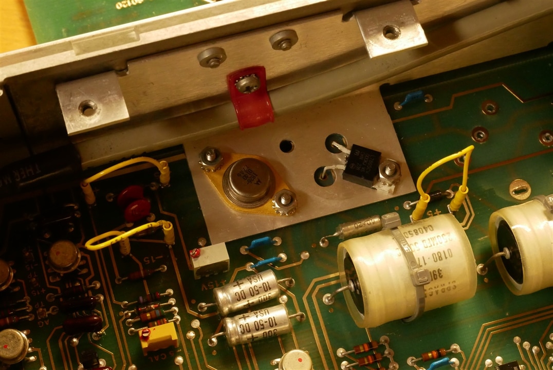
As you can see from the picture I bodged in a 7805 which got the 5V supply up but didn’t get the box working. But I though that making a TO3 shaped PCB with a regulator on it would be nice because this is not the first dead LM309 I’ve seen.

At first I was thinking of a linear regulator but looking on the web I found a design using a switching regulator. It was done a long time ago and used a rather dated switcher. While I was looking an email flyer form Linear Technology/Analog Devices turned up promoting their Silent Switcher 3 parts. These aren’t quite right for my intended spec (won’t take a high enough input voltage) although otherwise very good. So my design is going to use a Silent Switcher 2 part – the LT8640S.

And I’m using Kicad 8.0 to design the board.

First Impressions of KiCad

I bought some books (two, KiCad Fundamentals and Projects and KiCad Advanced Projects and Recipes both by Peter Dalmaris (on offer from Elektor as a bundle !)

I did not read all 590 pages of the Fundamentals before starting !

I dipped and then got on with it.

My biggest problem with KiCad is that it isn’t Easy PC. When you have 20 years experience with some software anything else is bound to feel a bit weird.

The schematic editor isn’t too hard to get used to but I found the part chooser a bit of pain. I was able to find a symbol and footprint for the LT8640s (on SnapMagic) quite easily and rather less easily add it to the library. This later cause a bit of a problem but it was the symbol not KiCad which I think was wrong.

Anyway – it wasn’t that hard to get a schematic done.

image

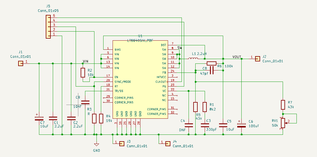
Translating to a PCB and placing that was OK. This is an odd design in that some parts must be placed in just the right positions and linked with lots of vias to ground or with copper pours rather than tracks. High speed switchers just don’t work right if you ignore this.

It was quite slow going because I had to keep looking up how to do stuff -  but that was to be expected.

The SnapMagic schematic symbol has all ground pins and the 4 little unconnected corner pins on top of each other. I thought this was a KiCad thing and was a bit disappointed by it but when I realised that all that was wrong was a whole load of ground pins being placed on top of each other in the schematic symbol I was soon able to edit it into something sensible. What I can’t understand is how any one could have thought that was a good idea -  not all ground pins are the same – even though they may be linked inside the chip.

Back to the layout – KiCad was a bit easier that EasyPC at allowing me to add vias to the PCB footprint of the LT8640s.

I don’t like the manual routing -  the software still keeps trying to coerce the track into silly shapes. This may be the way I have things set up and I shall experiment more before whinging. I like to route with a snap grid and without 90 or 45 degree constraints and then to adjust things the way I like. I might well break some clearance rules and move things later.

One snag that bit me was trying to set the outline of the TO3. The first problem was that KiCad calls the board outline the “EdgeCut” layer -  logical enough but hard to find when you search for things like “outline”. I had to actually read the book a bit to find that one.

Then I hit a big snag – all the footprints from the library were making solder paste and solder mask apertures exactly the same size as the pad.

I spent the next two days on and off searching for a global way of setting a different default. I could easily change every pad on the board one at a time. I found several hits on the web that suggested that there is not global way to this and advised people to edit the PCB text file or write scripts. The index in the Dalmaris book is very week and while it does tell you in the book you won’t find it in the index.

Having done a good deal of cursing I returned to web searching and found what I needed. I’ll share it here in case it’s useful:

In PCB Editor click the Board Setup button.

Click Solder Mask/Paste under Board Stackup

Enter things for solder mask expansion and solder paste relative clearance.

image

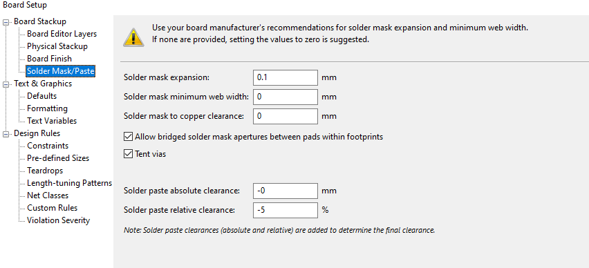
So of course KiCad lets you set these things globally and its actually in a sensible enough place !

image

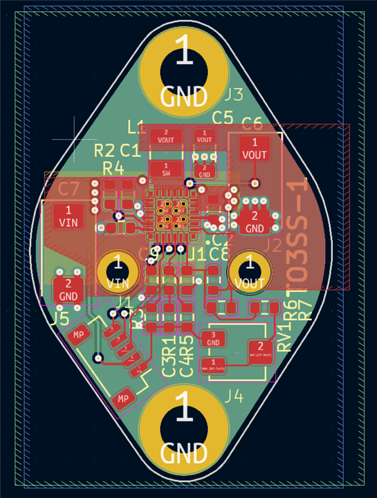
Now I could make the Gerber files and order the boards. It’ll be couple of weeks before they come back and I get bits on them and I can share some test results.

Conclusions

In conclusion – not too bad an experience. I’m not going to criticise because I haven’t used it enough to be sure that any problems I have are the software rather than me. But I didn’t hit any showstoppers. I think KiCad (on the basis of my limited experience)  is a competent offering in the low - to mid performance sector of the PCB CAD market.

I still paid for this year’s maintenance upgrade for Easy PC !

  • Sign in to reply

Top Comments

  • shabaz
    shabaz 10 months ago +2
    Hi Michael, I was going to point you toward my 50-minute quick-start video https://www.youtube.com/watch?v=5Be7XOMmPQE , but from that PCB screenshot is seems you don't need it. But maybe worth scanning…
  • shabaz
    shabaz 10 months ago in reply to Andrew J

    Hi! I found the same thing, that the default library parts leave a lot to be desired! : ) Even the plain errors aside, there are really silly things like TO-92 packaged parts default to a footprint where there are holes spaced 1.27 mm apart, when they could have been in a triangle with more sensible spacing. And massive SOT-23 hand-soldering version. Poor capacitor polarity marking on footprints. Ugly diode symbol in schematics with a line going through it as if it's shorted! 

    At least it is straightforward to "Save As" on an existing footprint or symbol, and rename it, and then correct it/improve it (whereas with EAGLE it was more hassle to do that).

    Also even the default line thicknesses for silkscreen are not great. I thicken to 0.127 mm instead of 0.1 mm, and increase text to 0.15 mm thickness at least.

    I also like that it's easy to tweak TQFP/QFN etc footprints by simply dragging pads to change their dimensions (and then group-selecting and just typing the new size, or moving as a group).

    The ability to have shaped pads is awesome. Plus non-circular holes (i.e. milled), for things like stamped metal connector terminals. That was such a headache to achieve in EAGLE.

    • Cancel
    • Vote Up 0 Vote Down
    • Sign in to reply
    • More
    • Cancel
  • Andrew J
    Andrew J 10 months ago

    I started with v5 and the frustrations you felt were the same as mine, particularly the drawing tools.  Trying to create an edge cut for a DB-9 (or whatever the letter is) was the Devil’s own job to get a neat curve that actually joined up and didn’t flag board errors.  At the time the on-line help was typically YouTube videos for earlier versions and I think v5 was a major interface change so there was a lot of translating.  What I’ve found is that over the versions I’ve worked out what works for me and then I, essentially, started again with libraries, footprints, paths, settings etc.  I didn’t have to struggle with coming from a different CAD software though, as KiCad was the first I used.  There’s some good tips in here: the only one I would add is that you MUST check library parts, esp. footprints.  I’ve found that there are often errors and it occurs in a high percentage - say circa 30% of parts.  At least creating symbols and footprints is easy.

    • Cancel
    • Vote Up 0 Vote Down
    • Sign in to reply
    • More
    • Cancel
  • michaelkellett
    michaelkellett 10 months ago in reply to Jan Cumps

    Another useful tip - thanks.

    MK

    • Cancel
    • Vote Up 0 Vote Down
    • Sign in to reply
    • More
    • Cancel
  • Jan Cumps
    Jan Cumps 10 months ago

    For the Vias, you can use "create array from selection". This is useful if you want to place a decent set of vias.

    • put one via 
    • select it, then right-click -> create from selection -> create array

    image

    • Cancel
    • Vote Up 0 Vote Down
    • Sign in to reply
    • More
    • Cancel
  • michaelkellett
    michaelkellett 10 months ago in reply to battlecoder

    Hello,

    Thanks for the tips !

    MK

    • Cancel
    • Vote Up 0 Vote Down
    • Sign in to reply
    • More
    • Cancel
>
element14 Community

element14 is the first online community specifically for engineers. Connect with your peers and get expert answers to your questions.

  • Members
  • Learn
  • Technologies
  • Challenges & Projects
  • Products
  • Store
  • About Us
  • Feedback & Support
  • FAQs
  • Terms of Use
  • Privacy Policy
  • Legal and Copyright Notices
  • Sitemap
  • Cookies

An Avnet Company © 2025 Premier Farnell Limited. All Rights Reserved.

Premier Farnell Ltd, registered in England and Wales (no 00876412), registered office: Farnell House, Forge Lane, Leeds LS12 2NE.

ICP 备案号 10220084.

Follow element14

  • X
  • Facebook
  • linkedin
  • YouTube