element14 Community
element14 Community
    Register Log In
  • Site
  • Search
  • Log In Register
  • Community Hub
    Community Hub
    • What's New on element14
    • Feedback and Support
    • Benefits of Membership
    • Personal Blogs
    • Members Area
    • Achievement Levels
  • Learn
    Learn
    • Ask an Expert
    • eBooks
    • element14 presents
    • Learning Center
    • Tech Spotlight
    • STEM Academy
    • Webinars, Training and Events
    • Learning Groups
  • Technologies
    Technologies
    • 3D Printing
    • FPGA
    • Industrial Automation
    • Internet of Things
    • Power & Energy
    • Sensors
    • Technology Groups
  • Challenges & Projects
    Challenges & Projects
    • Design Challenges
    • element14 presents Projects
    • Project14
    • Arduino Projects
    • Raspberry Pi Projects
    • Project Groups
  • Products
    Products
    • Arduino
    • Avnet & Tria Boards Community
    • Dev Tools
    • Manufacturers
    • Multicomp Pro
    • Product Groups
    • Raspberry Pi
    • RoadTests & Reviews
  • About Us
  • Store
    Store
    • Visit Your Store
    • Choose another store...
      • Europe
      •  Austria (German)
      •  Belgium (Dutch, French)
      •  Bulgaria (Bulgarian)
      •  Czech Republic (Czech)
      •  Denmark (Danish)
      •  Estonia (Estonian)
      •  Finland (Finnish)
      •  France (French)
      •  Germany (German)
      •  Hungary (Hungarian)
      •  Ireland
      •  Israel
      •  Italy (Italian)
      •  Latvia (Latvian)
      •  
      •  Lithuania (Lithuanian)
      •  Netherlands (Dutch)
      •  Norway (Norwegian)
      •  Poland (Polish)
      •  Portugal (Portuguese)
      •  Romania (Romanian)
      •  Russia (Russian)
      •  Slovakia (Slovak)
      •  Slovenia (Slovenian)
      •  Spain (Spanish)
      •  Sweden (Swedish)
      •  Switzerland(German, French)
      •  Turkey (Turkish)
      •  United Kingdom
      • Asia Pacific
      •  Australia
      •  China
      •  Hong Kong
      •  India
      • Japan
      •  Korea (Korean)
      •  Malaysia
      •  New Zealand
      •  Philippines
      •  Singapore
      •  Taiwan
      •  Thailand (Thai)
      • Vietnam
      • Americas
      •  Brazil (Portuguese)
      •  Canada
      •  Mexico (Spanish)
      •  United States
      Can't find the country/region you're looking for? Visit our export site or find a local distributor.
  • Translate
  • Profile
  • Settings
Arduino
  • Products
  • More
Arduino
Blog What would be your bare minimum on a Nano project PCB?
  • Blog
  • Forum
  • Documents
  • Quiz
  • Events
  • Polls
  • Files
  • Members
  • Mentions
  • Sub-Groups
  • Tags
  • More
  • Cancel
  • New
Join Arduino to participate - click to join for free!
  • Share
  • More
  • Cancel
Group Actions
  • Group RSS
  • More
  • Cancel
Engagement
  • Author Author: colporteur
  • Date Created: 8 May 2023 8:29 PM Date Created
  • Views 2443 views
  • Likes 13 likes
  • Comments 12 comments
  • arduino_development
  • arduino
Related
Recommended

What would be your bare minimum on a Nano project PCB?

colporteur
colporteur
8 May 2023

image

I’ve purchased the Arduino Nano holders above in the past for projects.

image

I have gone one step further and created PCB’s to hold a Nano and a JQ6500 sound module. I can share the KiCAD files if someone is interested. I reluctant to post them until I can improve the quality.

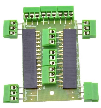
The ellipses shown on the boards proves that just because you can find a KiCAD footprints doesn't mean it is right. The ellipses on the left shows bow-legged pins because the footprint was wider than the actual module. The foot print dimension for the ellipse on the right were also off by 2.54mm. Live and learn.

After baring witness to Shabaz PCB design, I thought what would the E14 Community put as the bare minimum on a project board. I agree "it depends on what you want to do on the board." But I'm thinking there would be some general support even before the project starts. Things like power, protection, options.......

In the above project example. There is power I/P. I included a diode to prevent computer power feeding back into the power supply. I'm thinking maybe a 5V power supply. My design has the JQ6500 being supplied by the Nano. The example above uses 12VDC I/P. The 5V PS used in Shabaz design would be great on this board. Note my design doesn't have any filter capacitors that are see on other PCB's.

I'm currently working on a single Nano multi-function animation PCB. The board would have option to support light, sound and motion. The light would be LED's, the sound is the JQ6500 module and the motion would be some type of motor control. I'm currently thinking 5V servo but that is expanding. The board above supports a MOSFET module to drive a 12V load. There is a input to trigger the Nano with a button and speaker pins. 

I'm trying to get the model railroad community I play in, interested in microcontroller animation. If there was a small inexpensive PCB that allowed them to dabble in Arduino code to create simple animations, Lights coming on in a building. a car horn honking or a door opening on a building (i.e. light, sound and motion) maybe it would generate some interest. 

I'm curious what are your bare minimums for a Arduino project type board?

  • Sign in to reply
  • shabaz
    shabaz over 2 years ago

    Hi Sean,

    I think the board is generally fine, it has all the important bits like screw holes, reasonable thickness traces and even some protection with a diode to prevent reverse polarity damage, silkscreen labels to help identify connections.

    Probably the main issue as you say is that the online component footprints were not correct so that the connections to the Nano were splayed.

    I usually create my own part footprints, and keep calipers nearby while working, to double-check anything if I can't find the measurements in datasheets.
    If you've not created custom footprints yet with KiCad, then that is recommended, it will be the thing that will make the biggest improvement for projects.

    I'm biased since I created it, but I recommend the following video here for that, from time 15:33

    https://www.youtube.com/watch?v=5Be7XOMmPQE&t=1323s

    Here are my remainder comments:

    Circuit related:
    1. The circuit is very good, it is laid out well, and understandable. I'll paste it here, since it is worthwhile for newcomers to follow your layout and circuit, you should be comfortable with it : ) (Let me know if you prefer me to remove it, and I'll do that). I don't think I would change anything here, I would do it the same as you have done (with one small detail shown further below).

    image

    2. When interfacing the JQ6500 BUSY pin it's more conventional to have the resistor in the base. The screenshot here shows how to do it (the base resistor can be 1kohm, that is fine for turning on the transistor).

    image

    3. It's OK not to have any decoupling capacitors because the modules will have on-board capacitors already, but there's no harm with having space for a bulk decoupling capacitor on the board, for instance 10uF or so. You might want a slightly higher value capacitor (e.g. 47uF) since the JQ6500 module might have quite variable current demand when it is playing sounds.

    4. Sometimes I deliberately put a resistor in series into GPIO connections, even if it is not needed. That is handy for any connections that you're not sure of, so that they can be isolated when testing. Using (say) a 1kohm resistor (or lower resistance if required) can be handy if there's a risk that the GPIO might be accidentally set to output, if it is supposed to be input. I don't think that is relevant for this circuit, I'm just mentioning it for the times it may be needed.

    5. A fuse or polyfuse can be handy on boards, but I'm not sure I would use one on this board, since there's not much to go wrong, and it would be cheaper to replace a part than to place a fuse or polyfuse on every board

    6. Sometimes it is good to bring out a few unused GPIO pins to a pin header, in case any future uses come up.

    PCB related:
    1. As mentioned, the component footprints are better done (or verified) by yourself than trusting online ones. A shortcut is to copy an existing known good footprint and modifying it. In any case, for typical modules, it is easy to create a footprint because the pads will be all on a simple 2.54mm pitch (usually).

    2. The KiCad default silkscreen is a bit thin, so it is good that you're using 0.15mm thick text, rather than the default 0.1mm. Increasing the text size to 1.2mm x 1.2mm instead of the default 1 x 1mm can help improve visibility too.

    3. Text that is readable in one direction (i.e. no sideways text) is good, but it's not always possible.

    4. Great to see you've added lots of useful text labels. With the new KiCad 7, inverse text is also possible, it is an option within the normal text entry window.

    5. Personally I don't draw Edge.Cuts circles to create drill holes. It is better (I think) to just place mounting holes in the schematic, and assign a Mounting Hole footprint to that (there is a whole range of them in KiCad, for all popular hole sizes). I think the PCB manufacturers will prefer it too.

    6. When laying down traces, I don't bother routing the 0V (GND) connections, since that can all be handled with a ground plane. To create a ground place, use the "Add Filled Zone" icon (it is a blue icon) and draw a rectangle the same size (or slightly smaller) than the PCB. You'll see the option to select the signal you wish it to be, so you can select 0V (GND) there. To refresh the plane, just press the 'B' key whenever you need to. It's up to you whether the top layer or the bottom layer is the main ground plane (the filled zone can be set to both top and bottom layers simultaneously, which is useful, because of point 7 below).

    7. When laying down traces, I generally try to do it all on one layer, and only using the other layer for very short traces. Then, the ground plane can fill that entire generally empty layer. It's not necessary to put the ground plane on both layers, but it is worth doing for mechanical reasons (the board warps if there is more copper on one side than the other).

    8. Your traces are a good thickness. However, you can afford to make the traces thinner if they are not carrying a lot of power. For instance, all GPIO connections will be carrying just a few milliamps max. A good thickness for those traces is 0.25mm (you are using 0.5mm currently), and if you really need to make it thinner, then even 0.16mm is fine (not advisable to go thinner than that). I think your default trace should be 0.25mm, it will be equally reliable to the current 0.5mm traces.

    9. For higher current traces on the board, you're using 1mm thickness, and that is good, that seems reasonable.

    10. Not electrically important, but to make traces look nicer, I generally edit them after the first pass. If possible, I try to route traces out of pads to be square, i.e. not at a 45 degree angle if I can help it. It's more for satisfying OCDs than for any technical reason. So for instance, the trace below would be ripped up and replaced with a trace that is horizontal or vertical coming out of the pad.

    image

    11. Unless there's a special electrical reason, I don't like routing two traces out of a pad, and instead prefer to route a second trace off any position on the first trace if you see what I mean. 

    12. Not relevant for this board, but if there are buttons or LEDs, then I usually try to place them on round millimeter co-ordinates, to make life easier when drilling holes in enclosures.

    13. Board name and revision number are great to have on a board.

    14. Sometimes I'll label connections on both sides of the board, in case it helps when troubleshooting. Not essential always.

    • Cancel
    • Vote Up 0 Vote Down
    • Sign in to reply
    • More
    • Cancel
  • scottiebabe
    scottiebabe over 2 years ago

    I enjoyed reading this blog:

    image

    https://andrew-sterian.squarespace.com/10-ways-to-destroy-an-arduino 

    Perhaps there may be some inspiration within.

    • Cancel
    • Vote Up 0 Vote Down
    • Sign in to reply
    • More
    • Cancel
<
element14 Community

element14 is the first online community specifically for engineers. Connect with your peers and get expert answers to your questions.

  • Members
  • Learn
  • Technologies
  • Challenges & Projects
  • Products
  • Store
  • About Us
  • Feedback & Support
  • FAQs
  • Terms of Use
  • Privacy Policy
  • Legal and Copyright Notices
  • Sitemap
  • Cookies

An Avnet Company © 2026 Premier Farnell Limited. All Rights Reserved.

Premier Farnell Ltd, registered in England and Wales (no 00876412), registered office: Farnell House, Forge Lane, Leeds LS12 2NE.

ICP 备案号 10220084.

Follow element14

  • X
  • Facebook
  • linkedin
  • YouTube