element14 Community
element14 Community
    Register Log In
  • Site
  • Search
  • Log In Register
  • About Us
  • Community Hub
    Community Hub
    • What's New on element14
    • Feedback and Support
    • Benefits of Membership
    • Personal Blogs
    • Members Area
    • Achievement Levels
  • Learn
    Learn
    • Ask an Expert
    • eBooks
    • element14 presents
    • Learning Center
    • Tech Spotlight
    • STEM Academy
    • Webinars, Training and Events
    • Learning Groups
  • Technologies
    Technologies
    • 3D Printing
    • FPGA
    • Industrial Automation
    • Internet of Things
    • Power & Energy
    • Sensors
    • Technology Groups
  • Challenges & Projects
    Challenges & Projects
    • Design Challenges
    • element14 presents Projects
    • Project14
    • Arduino Projects
    • Raspberry Pi Projects
    • Project Groups
  • Products
    Products
    • Arduino
    • Avnet Boards Community
    • Dev Tools
    • Manufacturers
    • Multicomp Pro
    • Product Groups
    • Raspberry Pi
    • RoadTests & Reviews
  • Store
    Store
    • Visit Your Store
    • Choose another store...
      • Europe
      •  Austria (German)
      •  Belgium (Dutch, French)
      •  Bulgaria (Bulgarian)
      •  Czech Republic (Czech)
      •  Denmark (Danish)
      •  Estonia (Estonian)
      •  Finland (Finnish)
      •  France (French)
      •  Germany (German)
      •  Hungary (Hungarian)
      •  Ireland
      •  Israel
      •  Italy (Italian)
      •  Latvia (Latvian)
      •  
      •  Lithuania (Lithuanian)
      •  Netherlands (Dutch)
      •  Norway (Norwegian)
      •  Poland (Polish)
      •  Portugal (Portuguese)
      •  Romania (Romanian)
      •  Russia (Russian)
      •  Slovakia (Slovak)
      •  Slovenia (Slovenian)
      •  Spain (Spanish)
      •  Sweden (Swedish)
      •  Switzerland(German, French)
      •  Turkey (Turkish)
      •  United Kingdom
      • Asia Pacific
      •  Australia
      •  China
      •  Hong Kong
      •  India
      •  Korea (Korean)
      •  Malaysia
      •  New Zealand
      •  Philippines
      •  Singapore
      •  Taiwan
      •  Thailand (Thai)
      • Americas
      •  Brazil (Portuguese)
      •  Canada
      •  Mexico (Spanish)
      •  United States
      Can't find the country/region you're looking for? Visit our export site or find a local distributor.
  • Translate
  • Profile
  • Settings
Arduino
  • Products
  • More
Arduino
Arduino Forum LX-328 - 8 Bit Digital Logic Processor with two ATmega328P MCU's
  • Blog
  • Forum
  • Documents
  • Quiz
  • Events
  • Polls
  • Files
  • Members
  • Mentions
  • Sub-Groups
  • Tags
  • More
  • Cancel
  • New
Join Arduino to participate - click to join for free!
Actions
  • Share
  • More
  • Cancel
Forum Thread Details
  • Replies 22 replies
  • Subscribers 394 subscribers
  • Views 2114 views
  • Users 0 members are here
  • avr
  • atmega328
  • avr32
  • arduino
  • atmel
Related

LX-328 - 8 Bit Digital Logic Processor with two ATmega328P MCU's

iexpress
iexpress over 10 years ago

Hi Everyone!


I've been making a digital logic processor that has two ATmega328p MCU's on-board.


So far, I have the unit working through USB using a USB CDC protocol and have the

board processing digital logic through 7400 series logic.


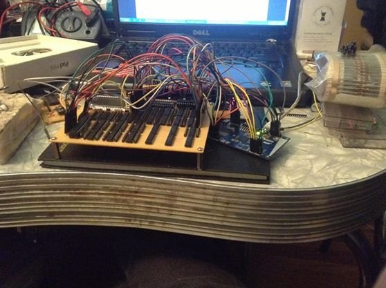
I just got the firmware programmed into the MCU's today using a UC3A3 Xplained as the ISP through SPI


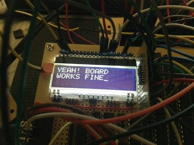
The board also has an LCD display, and I've started programming up a game for it called Super Micro Man

where the character is one character in size. https://www.youtube.com/watch?v=WD7Nmx1yU0E


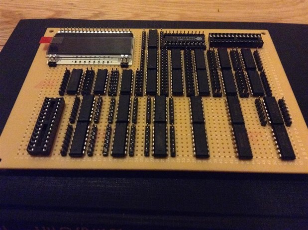
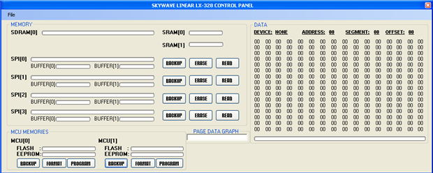
Details and Specs for my LX-328 board are:


Two ATmega328p MCU's running on their internal RC oscillators.


Two of each: AND, NAND, XOR, XNOR, OR, NOT, and NOR gates for comparing 2 bytes at a time and giving one byte output that is captured into a corresponding 74hc165 shift register.


Two dual 2-4 line decoders

Nine 74hc165

Three 74hc164


Electronic Assembly DOGM163S-A 3 line FSTN display.


Four AT45DB651E 64mbit Adesto DataFlash on two plugin cards.

Two 64k x 1 Cypress 7Y7C187-35PC SRAM


Here is a demo video showing one of the MCU's working right after I uploaded firmware and bootloader to the blank MCU: http://youtu.be/KezzU8PZMIc


I've also attached a document describing how to program the ATmega328(p) manually through ISP with SPI from another MCU.

You simply redirect the opcodes to the target from the host MCU through USB with ChipSelect on the target's Reset pin.


Here's a brief on what the board does and how it is working the digital logic internally: https://www.youtube.com/watch?v=no6mcuZ7e48

imageimageimageimage

Attachments:
ATmega328CompleteProgrammingGuide.rtf
  • Sign in to reply
  • Cancel

Top Replies

  • toxxn
    toxxn over 10 years ago in reply to iexpress +1
    Communication over internet between two of these would be phenomenal idea, especially for a Mini DIY kit like I mentioned above. This could allow two or more boards to chat with one another or even play…
  • toxxn
    toxxn over 10 years ago in reply to iexpress +1
    The NES was a little more advanced, especially with custom made components and the time period which separates basic 8-bit computers and the NES is pretty significant. There is not really any reason to…
  • toxxn
    toxxn over 10 years ago in reply to iexpress +1
    I prefer a nice appearance myself, not only for as you mentioned, making it easy to maneuver, but also because I like ascetics in keeping a clean and crisp project. Appearance is not always everything…
Parents
  • Robert Peter Oakes
    Robert Peter Oakes over 10 years ago

    I am curious, What is it your trying to do with this, you don't say


    All the logic your replicating in the 74 series TTL chips is available in the ATMEGA328's already so I'm not sure of your goal


    Thanks


    Peter

    • Cancel
    • Vote Up 0 Vote Down
    • Sign in to reply
    • Cancel
  • toxxn
    toxxn over 10 years ago in reply to Robert Peter Oakes

    Not sure of it intended function overall, but if I had a guess, I would say a homemade 8-bit computer of his own design. It looks to be a more complex TTL CPU complete with his own upgrades, which wonderfully demonstrates the use of simple logic gates, buffers, a binary adder, registers, multiplexors, decoders, flip-flops, and more. 7400 IC's are very common in TTL CPU projects, so it is interesting seeing this approach to say the very least.


    Jason, could you share a little more about it and it intended function(s)?


    Thanks,

    Cory

    • Cancel
    • Vote Up 0 Vote Down
    • Sign in to reply
    • Cancel
  • iexpress
    iexpress over 10 years ago in reply to toxxn

    Great guess Cory. The board is an 8-bit computer. Granted modern MCU's and CPU's handle logic internally, but I wanted to pose a challenge to myself to see if I could get something like this working.


    This is my first hardware project but I've added on a bunch of SPI components, each on their own dedicated line. The 64k x 1 SRAM is unique, and nicely, I am reading and writing to it using basic gpio functions while using adc pins for reading. In all data is handled by pin toggling.


    The board has one 8-bit input and an 8 bit output. Depending on which custom opcode comes in through the input 74hc164, one MCU handles which register receives the next incoming byte, and then it sends data on it's way to the appropriate logic gate. I have it sending the bytes out to all gates at the same time, but parallel loading one of nine 74hc165's at a time. When one is loaded, all the other output registers are 0x00 and have no effect on the one output register that has actual data.


    The second atmega328p handles peripheral IO, such as saving data to the four SPI flash roms, writing flash or sending data out through 8 channels or reading data into any of the 8 inputs.


    Even though I am more of a VB.Net programmer, it helped to understand what the C language was for. All of the components are working, even the LCD display. The hardest thing for me to do was program the application and bootloader code into the MCU flash manually by decyphering the Intel hex files to get the data and then start writing data to the appropriate locations in flash.


    Trouble is, I still don't have a connection to the PC for updating firmware on the MCU's so I can use the ISP interface at any time to update the program code. I do have a USB CDC connection with a UC3A3 Xplained evaluation board connected to the PC to run programming in real time in a sort of debug mode, but the opcode interrut language is a bit complicating because the unit listens for hex chars, then takes an action per letter it receives.


    For this board, the commands are 4 bit meaning 1 byte = 2 commands except when it requests data entry which is fed into the unit by keyboard on a host PC. You can think of the input as an SPI connection with clock and data line. implementing SPI with GPIO is a matter of toggling the data and clock pins in the right order. In my first attempt, all the values coming from SPI devices were multiplying the bytes by 0x02, even the shift registers all because I toggled the clock line first before checking if the corresponding adc pin was high before issuing clock.


    It was a matter of gpio_set_gpio_pin() and  gpio_clr_gpio_pin() functions where one pin is assigned SCK, MISO and MOSI along with a chip select line Per device. 8 data out lines, 8 data input lines, 4 chip selects, 8 clock lines and a 4 bit address bus that handles writing data to the SRAM just by setting an address.


    I gave the board 16 priliminary opcode instructions 0-F

    They set a uint8, uint16 and uint32 for SDRAM and SRAM data and addresses, select chips, write data, and read data.


    I'm definitely working on putting a user guide together, but in debug mode, what could be easier than just typing in hex chars to make the board do something.


    For example, if I wanted to read a byte from SPI Flash, I would select one of four. Selecting one deselects the others. I would enter:

    C10D190000900009000090B03

    C1 selects chip at location C1

    0D1 sets uint8 D1

    90 sends the uint byte D1 to the spi chip on C1 (SPI0)

    followed by 3 0x00 bytes sent to the chip on C1

    B0 reads a byte from SPI0 that is on C1

    3 prints the hex value of the byte read.

    C0 unselects all SPI chips setting the CS lines high.


    I could then store it in a temp 74hc165 by sending it with the 96 command which is Output Data Channel 7.

    9 means output while the following hex char tells it which channel to export the bye at 0-F although I was currently only using outputs 0-7.

    97 is write byte to LCD display. It's pretty unique. 0EE97 = set uint8 EE and send it to the LCD display.


    I'll definitely make a list of opcode commands. At the rate of developement, the list can continue of acceptable commands. In debug mode, the board listens for chars with scanf() then converts them into numbers.


    Outside debug mode, the whole process is automated rather than taking manual typed data entry. I can load data into ram from flash and even from MCU EEPROM by placing one MCU in ISP mode to get data with the other Atmega. We have Twice the power with two MCU's.


    I'll certainly be giving updates, maybe give this thing micro sdcard. Maybe making a pluging card for it as I have the SPI flash. Maybe create universal memory where interchangeable SRAM, Flash and FRAM cards could be used if the cards had the same ponout. Maybe use 8soic components. It's all very exciting.


    I Might even give this thing an R2R DAC for playing 8-bit audio. It is coming along nicely. I would consider things like IDE or compact flash but spi seems to be very stable with the unit.


    Glad you like the project. Feel free to check out my videos from the links I have posted in the topic above.

    I'll be giving updates the more features I can add on. Maybe I can even create a sort of command prompt for it. I gave it an OS name, Lilac and model number LX-328 to correspond with 32 MB of SPI flash and 8 bit operation.


    The first sixteen opcodes are 4-bit so one byte has two instructions in it. There is also an extended opcode list accessed by 0xF and then a set of another sixteen. It can keep going. The 16 and 32 bit variables are used to set the SDRAM address while the uint16 = uint8 to fill up the 16 bit SDRAM data with MSByte set to 0x00 per address location.

    • Cancel
    • Vote Up 0 Vote Down
    • Sign in to reply
    • Cancel
  • toxxn
    toxxn over 10 years ago in reply to iexpress

    Thank you for all the provided information Jason!


    When you gave the example of making it read bytes from the SPI Flash using Hex it honestly reminded me of the Apple 1 computer developed by Steve Wozniak back in 1976.

    I love your take on the 8-bit computer however and I like seeing these kinds of projects because there is always something new someone can add that just makes it that much more special while still keeping it what it is. I am defiantly interested in checking out updates you make on this project and I will certainly check out the videos you provided.


    What are your plans for connecting it via USB for updating the firmware rather than using an evaluation board?

    You mentioned possibly adding Micro SD and 8-bit Audio, are there any other additions you might be making, such as external display options, basic camera/ printer functions similar to that of the Gameboy camera/ printer for example, possibly analog support or another option for controller support for 8-bit games for example something similar to that of the Atari 2600 joystick?

    • Cancel
    • Vote Up 0 Vote Down
    • Sign in to reply
    • Cancel
  • iexpress
    iexpress over 10 years ago in reply to toxxn

    Might not be too hard expanding IO. I started making a couple games for the onboard lcd display which is pretty fun. Reading button presses might be fairly easy to implement. Perhaps I could give it an SPI color display, might have to search for the shift registers with latch to do some parallel output but still stick to the SPI standard. Audio might not be a problem, I made an 8 bit DAC once before but there just might be a 7400 series DAC, and even a VGA or composite video chip.


    USB-wise, I am using VB.Net to open the com port and can read/write data having full control over the board in real time sending hex chars to the board.


    I'll definitely keep everyone updated. Maybe even make a mini model of this board later on, possibly on shortrun PCB.


    Thanks!

    • Cancel
    • Vote Up 0 Vote Down
    • Sign in to reply
    • Cancel
  • iexpress
    iexpress over 10 years ago in reply to toxxn

    It could even be fun giving the board internet access through USB where the VB.Net app could send data across the internet talking with another like-unit if there were two boards. Could be useful for real-time messaging or data transfer and could be very secure with the range of logic gates the data could go through.

    • Cancel
    • Vote Up 0 Vote Down
    • Sign in to reply
    • Cancel
  • toxxn
    toxxn over 10 years ago in reply to iexpress

    I think it would be pretty awesome to add basic button inputs for 8-bit gaming purposes simply to add another twist to 8-bit computer projects such as this.


    As for Audio I have seen an example of i2s DAC with Class D Output which was an entry in a 7400 contest. As it so happens I have the link handy, maybe it could be of some use.

    http://willhb.com/?p=155


    As for Video, you are in some luck. I know of the ADV7125. It has three separate high speed 8-bit video DACs with a standard TTL input interface. It has additional video signal options such as composite SYNC and BLANK as well. Might be a little more than what you need, albeit could be something to check into. Here is a spreadsheet of the ADV7125; http://www.analog.com/static/imported-files/data_sheets/ADV7125.pdf


    A mini DIY kit of this would be an awesome project for anyone looking to play with and/or learn digital logic not to mention the opportunity for someone to build their own little 8-bit computer. I could see something like this being on kickstarter or even as a kit on sites such as E14 or Adafruit.


    Looking forward to seeing updates.

    • Cancel
    • Vote Up 0 Vote Down
    • Sign in to reply
    • Cancel
  • toxxn
    toxxn over 10 years ago in reply to iexpress

    Communication over internet between two of these would be phenomenal idea, especially for a Mini DIY kit like I mentioned above.

    This could allow two or more boards to chat with one another or even play 8-bit games together using the also mentioned button inputs idea.

    • Cancel
    • Vote Up +1 Vote Down
    • Sign in to reply
    • Cancel
  • iexpress
    iexpress over 10 years ago in reply to toxxn

    SUre, it could be feasible to make a small kit preloaded with firmware so all they have to do is plug it into USB and then use an app that does the data transfer and board control. aybe I can interface an NES controller port. I believe they are 8-bit, and could check for button presses. Maybe give the lcd display a command prompt or graphical user interface With several different options.


    There should be enough RAM and ROM. The SPI flash has two 256 byte data buffers each giving 2046 bytes SRAM scratchpad memory. Today I will probably finish up most of the Visual Basic.Net app. i'll have it access all memories, and then work having it keep track of where it puts data into flash using a sort of binary file. This way it would save space on the SPI flash. Create a small defragmenter for it when files are deleted but let the user defrag when they want. I guess that would be a memory controller. One of the goals might be to keep everything in binary so there are no gaps in flash or filesystems.


    Should have the majority of the board finished in a day or two, then can add onto it from there.

    • Cancel
    • Vote Up 0 Vote Down
    • Sign in to reply
    • Cancel
  • toxxn
    toxxn over 10 years ago in reply to iexpress

    You are correct the NES was 8-bit.

    The NTSC version had a 8-bit Microprocessor which ran at a 1.79 MHz clock rate, contained 2KiB of onboard work RAM, and 2 KiB of VRAM, 28bytes of pallette ram and 256 bytes of OAM for it's custom-made PPU (picture processing unit). The system supported up to 32 KiB of program ROM, which could be expanded by a process of bank switching. The games themselves varied in memory but the most common ran around 130-400KiB.

    • Cancel
    • Vote Up 0 Vote Down
    • Sign in to reply
    • Cancel
  • iexpress
    iexpress over 10 years ago in reply to toxxn

    I suppose it could be possible to put a PPU in the circuit for NTCS output along with a 6502 CPU for analog audio.

    They might be 5 volt but I think they could be controlled by a shift register. That might be fairly advanced though, it would be simpler to add an SPI based display. if there was a PPU in the circuit, some displays can take composite video as input. I could possibly create dynamic callobration where the delay value is in ram instead of rom, and could be changed by the microsecond.

    • Cancel
    • Vote Up 0 Vote Down
    • Sign in to reply
    • Cancel
  • toxxn
    toxxn over 10 years ago in reply to iexpress

    The NES was a little more advanced, especially with custom made components and the time period which separates basic 8-bit computers and the NES is pretty significant.

    There is not really any reason to go too complex with an 8-bit computer, however it is cool to see new ideas.

    • Cancel
    • Vote Up +1 Vote Down
    • Sign in to reply
    • Cancel
Reply
  • toxxn
    toxxn over 10 years ago in reply to iexpress

    The NES was a little more advanced, especially with custom made components and the time period which separates basic 8-bit computers and the NES is pretty significant.

    There is not really any reason to go too complex with an 8-bit computer, however it is cool to see new ideas.

    • Cancel
    • Vote Up +1 Vote Down
    • Sign in to reply
    • Cancel
Children
  • iexpress
    iexpress over 10 years ago in reply to toxxn

    Right on, it would be a little difficult to add those components. I'll keep building and programming to see about getting the current hardware working a bit better. I might take a break for a bit to think on the programming aspect. It is a little complicating, especially with the additional hex chars so data gets routed correctly. I'll be in touch soon.


    Currently, the specs are:


    0xC0 Unselect Selected SPI CS

    0xC1 SPI0 Chip Select

    0xC2 SPI1 Chip Select

    0xC3 SPI2 Chip Select

    0xC4 SPI3 Chip Select


    0x90 SPI0 MOSI uint8_t

    0x91 SPI1 MOSI uint8_t

    0x92 SPI2 MOSI uint8_t

    0x93 SPI3 MOSI uint8_t

    0x94 Write SRAM1 LSB Address Byte uint8_t

    0x95 Write SRAM1 MSB Address Byte uint8_t

    0x96 Shift Register MOSI uint8_t

    0x97 LCD Display MOSI uint8_t


    0xB0 SPI0 MISO uint8_t

    0xB1 SPI1 MISO uint8_t

    0xB2 SPI2 MISO uint8_t

    0xB3 SPI3 MISO uint8_t

    0xB4 reserved

    0xB5 reserved

    0XB6 Shift Register MISO uint8_t

    0xB7 SRAM1 MISO uint8_t


    0xD0 Deselects all addresses

    0xD1 AddressA SRAM1 MOSI

    0xD2 AddressB SRAM1 READ/WRITE

    0xD3 AddressC SRAM1 Chip Select

    0xD4 AddressD LCD Display RS DATA COMMAND


    0x0 Set uint8_t

    0x1 Set uint16_t

    0x2 Set uint32_t

    0x3 Set SRAM0 Address uint8_t

    0x4 Set SDRAM0 Address uint32_t

    0x5 Set SRAM0[Address] uint8_t

    0x6 Set SDRAM0[Address] uint8_t

    0x7 Increment SRAM0 Address with Wrap-Around

    0x8 Increment SDRAM0 Address with Wrap-Around

    0x9 Data Output uint8_t

    0xA Data Input uint8_t Mode 0: Clock, Data (multiply byte by two)

    0xB Data Input uint8_t Mode 1: Data, Clock

    0XC Chip Select uint8_t

    0xD SRAM1 Controller: 0x1 Write Data High, 0x0 Write Data Low, 0x3 Output Enabled, 0x2 not used.

    0xE Toggle LCD Display RS Data/Command Pin

    0xF Extended Opcode List


    0xF0 Increment SRAM1 Offset with Wrap-Around

    0xF1 Increment SRAM1 Segment with Wrap-Around


    And tons more to come.

    • Cancel
    • Vote Up 0 Vote Down
    • Sign in to reply
    • Cancel
  • toxxn
    toxxn over 10 years ago in reply to iexpress

    It is always good to take a break once in awhile. Programming can get pretty stressful at times and there is no reason to overwork yourself. : )

    • Cancel
    • Vote Up 0 Vote Down
    • Sign in to reply
    • Cancel
  • iexpress
    iexpress over 10 years ago in reply to toxxn

    I spent the day rewiring the board twisting groups of wires together into braids to make the appearance a little nicer. It also helped to make the board easier to get around. I placed the MCU's on the SPI bus so now the MCU's can be selected in ISP mode directly. I might hand it a boot option where users can select which device they'd like to boot from, like SPI0-SPI3, EEPOM0-EEPROM1(MCU EEPROM). This might come in handy being able to select the MCU's to read and write from EEPROM contents without disturbing each MCU's flash. I can give them the option to Save EEPROM so upgrading flash won't format the EEPROM data. There might not be a need to update flash firmware, but with access to the MCU flash, some users might be enticed to update but it could make the board inoperable. For this, I can create forbidden opcodes unless the user is in some sort of Administrator mode. This could be accomplished by a boolean, IsAdmin. If IsAdmn == true.... I'll be creating the command prompt over the next few days. There will be 6 devices the user can boot from, any of the SPI loading from 0x0000 or from either MCU EEPROM. With a list of opcode instructions available to the user, they can freely develop their own operating system contolling data flow. The other thing is you could still read and write to the boot device. Perhaps the bootloader could be 256 or 512 bytes. 1 or 2 pages in the boot section of the device. Maybe I could place a byte at the end of EEPROM in one of the MCU's that shows which device to boot from, and how many 256 byte pages the bootloader is since it can be written to 100,000 times. High 4 bits show which device to boot from, and Low 4 bits show how many pages the bootloader is. Guess it could have up to 16 pages of 256 bytes available in each page.

    • Cancel
    • Vote Up 0 Vote Down
    • Sign in to reply
    • Cancel
  • toxxn
    toxxn over 10 years ago in reply to iexpress

    I prefer a nice appearance myself, not only for as you mentioned, making it easy to maneuver, but also because I like ascetics in keeping a clean and crisp project. Appearance is not always everything, but it really does help.


    I like your idea of adding a boot option allowing the user to select which device they would like to boot from. I like having options rather than just being subjected to a single thing, if options are available. This is why if you use any one of my SD Cards for my Raspberry Pi's, you will find at least two OS options.. that is unless what I am working on requires only one, such as the Raspberry Pi arcade project I am working on.

    • Cancel
    • Vote Up +1 Vote Down
    • Sign in to reply
    • Cancel
  • iexpress
    iexpress over 10 years ago in reply to toxxn

    Was working on a control panel in Visual Basic.Net today to access all memories on the board. I'll be handing it an automated and a manual mode where manual mode would allow controlling the board through data entry entering hex chars, and the automated mode would operate automatically incrementing stack and instruction pointers. One more week and the majority should be finished. There's an SPI based display headed this way so I'll definitely integrate that into one of the SPI channels.

    image

    • Cancel
    • Vote Up 0 Vote Down
    • Sign in to reply
    • Cancel
  • clem57
    clem57 over 10 years ago in reply to iexpress

    Oh. This gives me an idea with what I am playing with! Windows programming hardware on remote boards. Love it. image


    Thanks,

    Clem

    • Cancel
    • Vote Up +1 Vote Down
    • Sign in to reply
    • Cancel
  • iexpress
    iexpress over 10 years ago in reply to clem57

    Yay! I'm very excited, but I've been controlling it in real time entering hex chars through the keyboard. With the hardware working, I can go ahead and create a way to increment and retrieve data from flash or either of the MCU's EEPROM. Also working to develop some sort of command prompt, but I'll probably have to make some custom peripherals for data entry if the board is used in standalone automated mode.


    The board should give beginners a chance to understand the 7400 series logic with the addition of SPI-based storage solutions.


    Creating a user guide might take about a week, but I'll cover everything from running the board in real time using the opcodes, to creating apps that run automatically from any of the storage devices on the board. Currently there are 6 non-volatile memories, but the SPI-Flash also has two 256 byte buffers a piece available to the user.


    Still not sure if there is a way to access MCU SRAM in ISP programming mode, but this is how I'll be having it access Flash and EEPROM.

    Perhaps the drive labels could correspond with the devices, SPI0:\ EEPROM0:\ etc.


    We'll get there, it'll take about a week to finish a bootloader but the user guide will even cover this.

    For updating MCU Flash, I'll just have the VB.Net app handle ISP programming in circuit through USB CDC.


    No more wondering how to get code onto the MCU's that are blank and don't have their own bootloaders.

    I spent a day or two understanding how bytes are written to the ATmega328P Flash, 2 bytes per address.

    Hex files show one byte per address, but the loading address is the first address shown in the hex file.

    From there, I can have the VB.Net app upload data into either of the MCU's.


    I also made them removable so they can be replaced and reprogrammed very quickly.


    image

    • Cancel
    • Vote Up 0 Vote Down
    • Sign in to reply
    • Cancel
  • toxxn
    toxxn over 10 years ago in reply to iexpress

    A new SPI display? Please do post a new picture after this has been integrated. I would love to see new changes as they are implemented.


    Good idea on making the MSU's removable.

    I have had a few ATmega's and even a couple 555 timers burn out on me. Having those DIP sockets really do prevent the tedious work of having to de-solder when this happens.


    As I mentioned before, boards like this are great educational pieces when learning not only 7400, but basic logic in general.

    • Cancel
    • Vote Up +1 Vote Down
    • Sign in to reply
    • Cancel
element14 Community

element14 is the first online community specifically for engineers. Connect with your peers and get expert answers to your questions.

  • Members
  • Learn
  • Technologies
  • Challenges & Projects
  • Products
  • Store
  • About Us
  • Feedback & Support
  • FAQs
  • Terms of Use
  • Privacy Policy
  • Legal and Copyright Notices
  • Sitemap
  • Cookies

An Avnet Company © 2025 Premier Farnell Limited. All Rights Reserved.

Premier Farnell Ltd, registered in England and Wales (no 00876412), registered office: Farnell House, Forge Lane, Leeds LS12 2NE.

ICP 备案号 10220084.

Follow element14

  • X
  • Facebook
  • linkedin
  • YouTube