I am interfacing Avnet AU board-15P(AES-AUB-15P-DK-G, Rev 01) with LVDS transmitter on it, to communicate with a external LVDS receiver through FMC connector. I observed that some pins of the FMC connector are mapped to HPIO capable signals and others are mapped to HDIO capable signals.
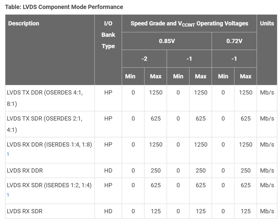
From the datasheet of Artix-Ultrascale+ FPGA, it is understood that HDIO signals maximum supported data rate is 250Mbps whereas HPIO capable pins support 2.5Gbps.
However, Assigning HDIO signals with lower data rate to FMC connector doesn't seem to be aligned with the FMC standard.
The basic requirement for our design is to have a interface that support LVDS transmission with data rate of at least 625Mbps.
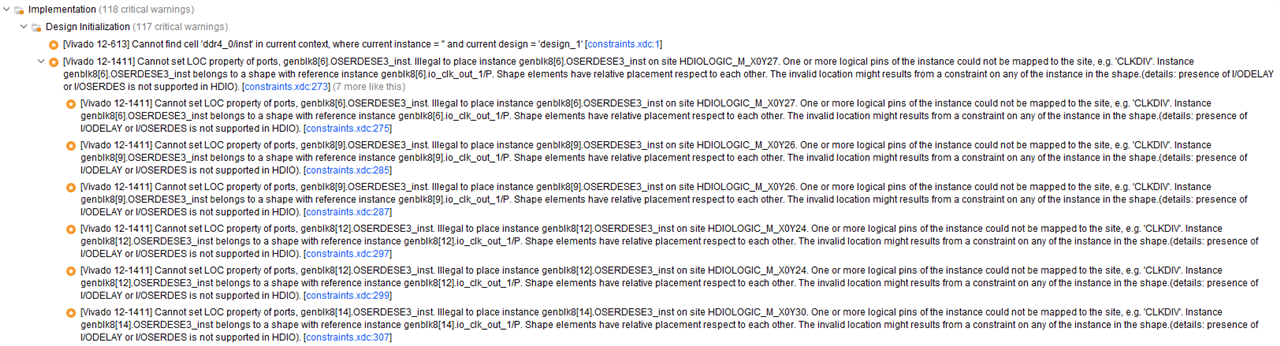
I can see a warning in vivado- v 2024.2 tool mentioning illegal placement on those pins. Even though this is a warning, I could see signal integrity issue in the output.
Some of the HDIO signals that are mapped to FMC are following pairs:
(H14, G14)
(J14, J15)
(J12, H12)
(E13, E12)
Attaching the warnings for reference:
Is there any way to have work around for this issue?