


- Beginning Schematic Capture
- Challenges of Schematic Capture
- Defining Variants within Altium, reasoning behind defining different builds
- Finalizing Schematics, Review process ect.
Schematic Capture can be considered a daunting task especially when you have had limited exposure to it and the tool set you plan on using. In our instance we wanted to use Altium for this schematic and PCB design capture. Being relatively new, I partook in a training course by Robert Feranec through FEDEVEL Academy in which I learned the basics of any Altium design including best practices, navigate the tool, setting variants, and PCB navigation. Everything I needed to get started. I would highly recommend attending one of Robert’s courses though FEDEVEL Academy if you want to learn about schematic and PCB development.
With this skillset obtained we began out schematic capture. We setup out project with seventeen schematic pages to properly organize out design in a logical and meaning way.
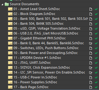
- Avnet Lead Sheet – This is the title page showing what revision and variant the schematic is showing
- Block Diagram – A Logical block diagram is provided on page two to show the system architecture
- Bank 500, Bank 501, Bank 502, Bank 503 – All the processor side of the SoC, including MIOs, SoC reference clocks, and JTAG/boot mode interface
- Bank 504, Bank 505 – DDR and GTR banks of the SoC
- uSD, QSPI, Voltage Translation – SD Card boot circuit, QSPI boot circuit, Click translation, and SYZYZY translation
- USB 2.0, JTAG_UART Micro USB – USB 2.0 host circuit, and JTAG/UART micro-USB interface
- Gigabit Ethernet PHY – Gigabit Ethernet PHY circuit including RJ45, magnetics, and MAC ID EEPROM
- Bank 0, Bank 44, Bank 65, Bank 66 – Banks of all high density and high-performance IO available on the SoC
- Switches, LEDs, Push Buttons – User IO, boot method switch, and status LEDs
- Bank Power, and Decoupling – Power banks of SoC including required decoupling capacitors
- LPDDR4 Device – 1GB LPDDR4 RAM circuit
- JTAG, UART – JTAG and UART circuit
- SYZYGY, Click Expansion – Click and SYZYGY add on expansion interfaces
- I2C_SPI sensor, power-on enable – I2C sensor, SPI sensor, power on and power sequencing circuits
- USB-C Power In – USB C power SINK circuitry
- Power Supplies – Main power supplies providing power to SoC and peripherals
- Back Page – Extra mechanical requirements such as bumpers, cables, heatsink, etc.
After setting up your schematic pages, you then begin your schematic capture which involves adding new components into your library. When it comes to adding components, it is very important to have checks and balance in addition a revision control system in place. This is in order to avoid making mistakes in component symbol and footprint creation which has the potential to add costly board spins if you are not careful. Work with your component management system and component engineer on this. In our case we are using Altium365 for this function. After you have your components added you can now begin and complete your schematic capture.
During your schematic capture, you will also want to start defining and updating your variant. For those who are unaware of what a variant is, it is a BOM management system in which you define which components are populated in your build. In some instances, you want the footprint of a component is populated but not the actual component. This is incredibly useful in testing our new interfaces using different circuitry. You populated you design in a know good circuitry for your prototypes along with your new circuit you want to test, assuming everything checks out with your new circuit you then depopulate your old proven circuit in production as it’s no longer needed.
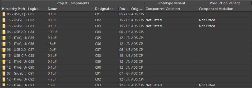
One instance we did this on the ZUBoard is we populated a USB C SINK circuit that negotiates USB C power to 15V VIN. In addition, we populated a 12V VIN barrel jack. We did this incase there was an issue with the USB C Power 15V VIN. We wanted to make sure that even if the USBC power in wasn’t working as expected we could still power the boards to complete validation of all other interfaces over the barrel jack power in. In many instances we also utilized 0ohm resistors to potentially populate different configurations, such as the MAC ID EEPROM & Ethernet PHY circuit. After your variants are completed, you then must utilize your DRC checks to potentially catch any schematic issues.
Now that your initial schematic is complete, you must now go through schematic design reviews in which you submit them to you colleagues to provide checks and balances to your design. Thus, must be done as you are your worst reviewer, you will overlook any minor mistake as you designed it and have tunnel vision on the design. Typically involving other engineers to review it brings up questions regarding why things were done a certain way in which you must take into consideration other individuals’ point of view and articulate why their recommendation or theirs is the best way of doing such a design. You must always take the others point of view into consideration for sake of getting the best design possible.
In addition to a standard schematic review make sure to work with your software resource to verify everything they need regarding interfaces is properly met. What I mean by this is how much DDR do they need, is the MAC ID properly interfaced to the system for your Ethernet PHY. Are you using the desired protocol addresses they are expecting in their software development? This provides a unique system level approach to your design.
Now that you have reviewed your schematic with your team, you are safe to proceed to the layout of your board. Tune in for the next blog in which I will go through this process with you.
Check out the previous and future blogs!
Link to Blog #2 - /products/devtools/avnetboardscommunity/b/blog/posts/zuboard-1cg-2-how-to-begin-system-architecture
Link to Blog #4 - Coming soon