element14 Community
element14 Community
    Register Log In
  • Site
  • Search
  • Log In Register
  • About Us
  • Community Hub
    Community Hub
    • What's New on element14
    • Feedback and Support
    • Benefits of Membership
    • Personal Blogs
    • Members Area
    • Achievement Levels
  • Learn
    Learn
    • Ask an Expert
    • eBooks
    • element14 presents
    • Learning Center
    • Tech Spotlight
    • STEM Academy
    • Webinars, Training and Events
    • Learning Groups
  • Technologies
    Technologies
    • 3D Printing
    • FPGA
    • Industrial Automation
    • Internet of Things
    • Power & Energy
    • Sensors
    • Technology Groups
  • Challenges & Projects
    Challenges & Projects
    • Design Challenges
    • element14 presents Projects
    • Project14
    • Arduino Projects
    • Raspberry Pi Projects
    • Project Groups
  • Products
    Products
    • Arduino
    • Avnet Boards Community
    • Dev Tools
    • Manufacturers
    • Multicomp Pro
    • Product Groups
    • Raspberry Pi
    • RoadTests & Reviews
  • Store
    Store
    • Visit Your Store
    • Choose another store...
      • Europe
      •  Austria (German)
      •  Belgium (Dutch, French)
      •  Bulgaria (Bulgarian)
      •  Czech Republic (Czech)
      •  Denmark (Danish)
      •  Estonia (Estonian)
      •  Finland (Finnish)
      •  France (French)
      •  Germany (German)
      •  Hungary (Hungarian)
      •  Ireland
      •  Israel
      •  Italy (Italian)
      •  Latvia (Latvian)
      •  
      •  Lithuania (Lithuanian)
      •  Netherlands (Dutch)
      •  Norway (Norwegian)
      •  Poland (Polish)
      •  Portugal (Portuguese)
      •  Romania (Romanian)
      •  Russia (Russian)
      •  Slovakia (Slovak)
      •  Slovenia (Slovenian)
      •  Spain (Spanish)
      •  Sweden (Swedish)
      •  Switzerland(German, French)
      •  Turkey (Turkish)
      •  United Kingdom
      • Asia Pacific
      •  Australia
      •  China
      •  Hong Kong
      •  India
      •  Korea (Korean)
      •  Malaysia
      •  New Zealand
      •  Philippines
      •  Singapore
      •  Taiwan
      •  Thailand (Thai)
      • Americas
      •  Brazil (Portuguese)
      •  Canada
      •  Mexico (Spanish)
      •  United States
      Can't find the country/region you're looking for? Visit our export site or find a local distributor.
  • Translate
  • Profile
  • Settings
Autodesk EAGLE
  • Products
  • More
Autodesk EAGLE
Blog Making a PCB in Eagle
  • Blog
  • Forum
  • Documents
  • Events
  • Polls
  • Files
  • Members
  • Mentions
  • Sub-Groups
  • Tags
  • More
  • Cancel
  • New
Join Autodesk EAGLE to participate - click to join for free!
  • Share
  • More
  • Cancel
Group Actions
  • Group RSS
  • More
  • Cancel
Engagement
  • Author Author: Workshopshed
  • Date Created: 8 Sep 2014 12:03 PM Date Created
  • Views 2296 views
  • Likes 3 likes
  • Comments 3 comments
  • pcb
  • 555
Related
Recommended

Making a PCB in Eagle

Workshopshed
Workshopshed
8 Sep 2014

In my previous post on Starting out with Eagle I followed Jeremy Blum's tutorial to build a 555 timer circuit using Eagle's schematic editor. I've now followed the next video and put together a PCB.


Before moving on from your schematic to PCB, I strongly advise running through the ERC or "Electrical Rule Check", this will tell you if you've done things like shorting the powersupply, left pins unconnected or in my case appear to have connected two nets but have actually just overlaped the lines.

image

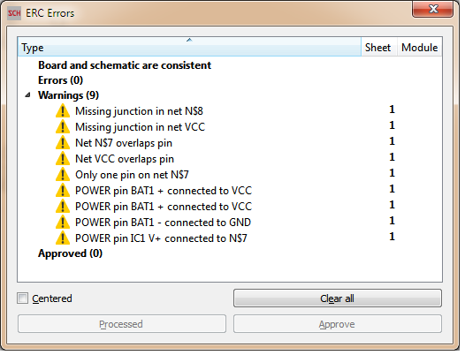
Here's the IC1 power pin zoomed in. When I moved the VCC net you'll see that it's not actually connected to the IC. I ended up deleting the VCC component, reconnecting the net and then rotating it.

                                           imageimage

The warnings about Bat+ and IC1 V+ connected to VCC could be "Approved" as those are the right connection. My battery has two different +V connections so those both needed wiring up which also was spotted by the ERC.

I managed to clear the errors and get on with designing the board. I have left the layout to emphasise these points.


image

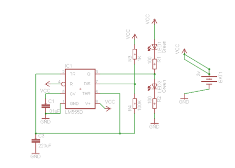
As mentioned above it's key to ensure your schematic is complete and fault free before working on the board design. Also the position of the components will make a big difference to how easy it is for you (or the auto-router) to route the board.


I used Jeremy's idea of adding a polygon as a ground plane on the bottom layer. This can simplify the design but can also complicate the workflow as you often have to "ratsnest" the polygon to generate the gaps and holes around the components. Watch Tutorial 2 to see that in action. The rats nest option is also very useful when you are ripping up tracks after moving or rotating components which I did several times.


I did try the auto router a few times and it did come up with a clever single sided board however it managed that with traces between pins and under the resistors and LEDs. I don't mind traces under the larger components (see board design below) but I thought for a default setting that was a bit strange. I've not had enough time to work with the autorouter to get it to produce designs I would be happy with.

image

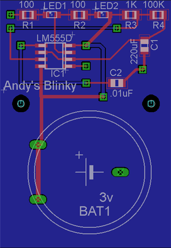
The vias are added automatically when your route is on multiple layers although I found I had to change the default drill size to pass the DRC (design rule check). As with the ERC it's worth running this check as it will let you know if you have overlapping components, traces that are too close together or a silly error such as drilling the same hole 3 times with different sized drills.


My final tip would be to descide on a suitable track size up front, I found it a pain to change these retrospectively, it might be possible to multiselect traces but I've not found a way to do that yet. I did experiment with making the power traces larger on my board but have ended up with a bit of a mix of sizes. I also can't seen to find a metric option for drill and trace sizes as I find the old imperial measures a bit cryptic.


It did take me some time to come up with a layout I was happy with although even now there are things I'd change but I believe I have a working board design. I'll review that after watching the 3rd tutorial.

  • Sign in to reply
  • Workshopshed
    Workshopshed over 10 years ago

    The answer to setting to mm found by Joop14 type "grid mm" in the command prompt.


    Metric?

    • Cancel
    • Vote Up 0 Vote Down
    • Sign in to reply
    • More
    • Cancel
  • Workshopshed
    Workshopshed over 10 years ago in reply to shabaz

    Thanks, that net classes sounds useful, more reading needed...

    • Cancel
    • Vote Up 0 Vote Down
    • Sign in to reply
    • More
    • Cancel
  • shabaz
    shabaz over 10 years ago

    Hi Andy,


    Good stuff! And its good advice on the ERC too. It always gets me out of trouble, invariably it will spot stuff I'd missed or forgotten even on small designs.


    Regarding the wire thickness, it is possible from the schematic to put wires into 'net classes' (and set up the classes from Edit->Net Class menu option) and that is useful for (say) power traces as you say. It's still not perfect (since some parts may not need to be thickened, e.g. a supply line connected to a 100k resistor wouldn't need a thick line) but that could be thinned later.

    • Cancel
    • Vote Up 0 Vote Down
    • Sign in to reply
    • More
    • Cancel
element14 Community

element14 is the first online community specifically for engineers. Connect with your peers and get expert answers to your questions.

  • Members
  • Learn
  • Technologies
  • Challenges & Projects
  • Products
  • Store
  • About Us
  • Feedback & Support
  • FAQs
  • Terms of Use
  • Privacy Policy
  • Legal and Copyright Notices
  • Sitemap
  • Cookies

An Avnet Company © 2025 Premier Farnell Limited. All Rights Reserved.

Premier Farnell Ltd, registered in England and Wales (no 00876412), registered office: Farnell House, Forge Lane, Leeds LS12 2NE.

ICP 备案号 10220084.

Follow element14

  • X
  • Facebook
  • linkedin
  • YouTube