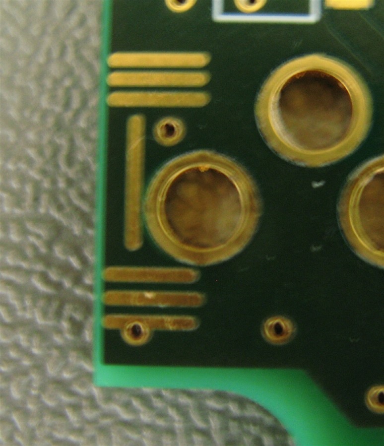
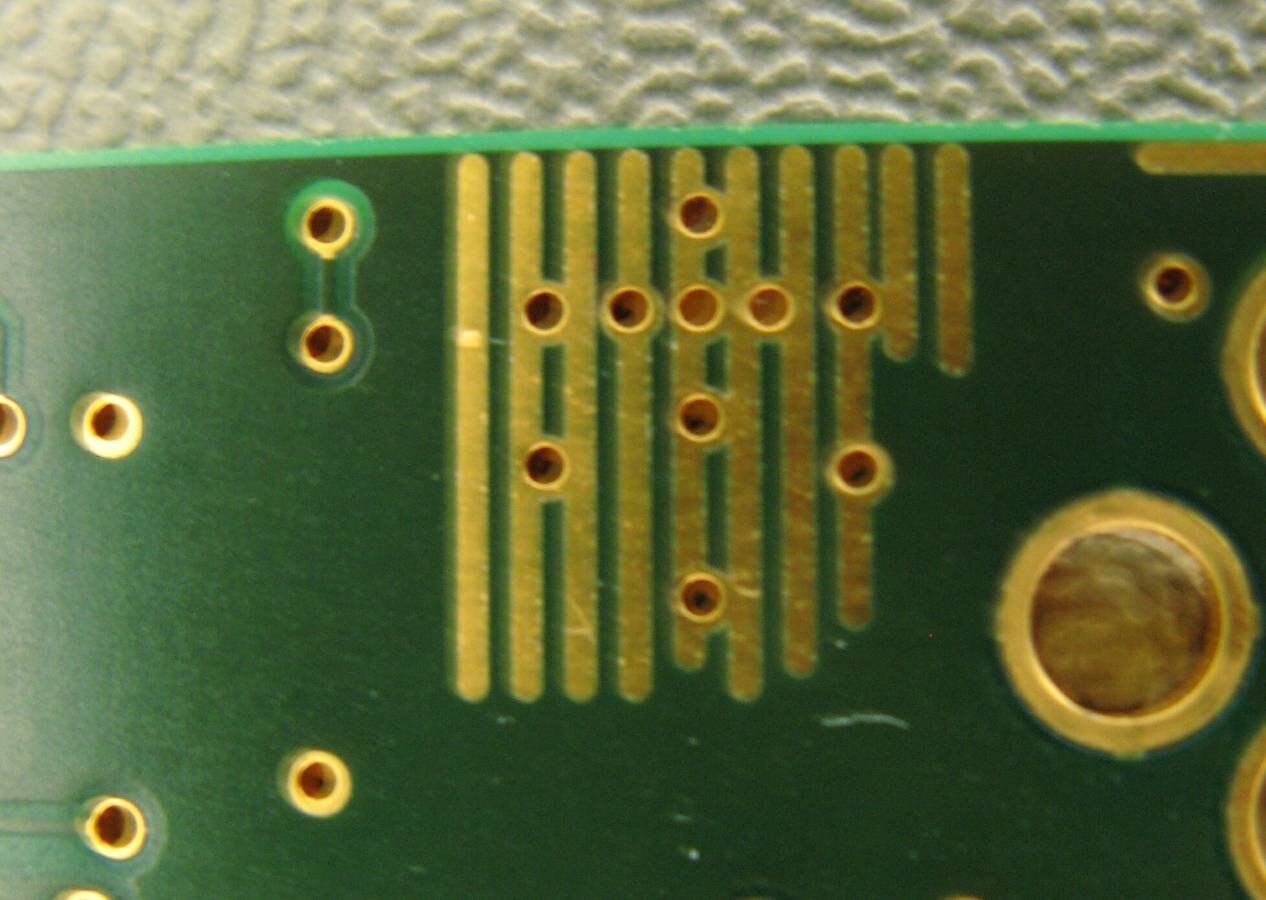
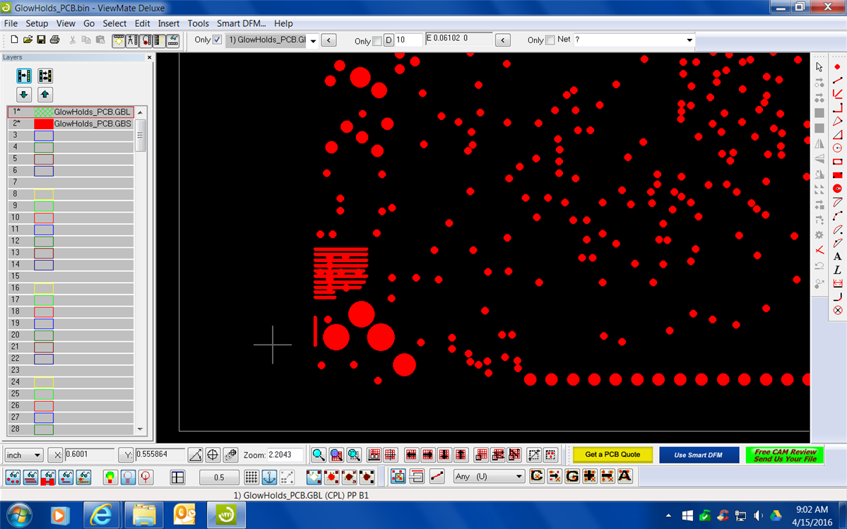
I have an Eagle 7.5 PCB that I am working on. The solder mask layer on top and bottom have some very strange line openings. I do not know how they got there, nor do I know how to remove them. Please see the images below. They don't seem to be part of any component as if I move the component, they are still there. Can someone tell me how to remove these? Thank you!