element14 Community
element14 Community
    Register Log In
  • Site
  • Search
  • Log In Register
  • Community Hub
    Community Hub
    • What's New on element14
    • Feedback and Support
    • Benefits of Membership
    • Personal Blogs
    • Members Area
    • Achievement Levels
  • Learn
    Learn
    • Ask an Expert
    • eBooks
    • element14 presents
    • Learning Center
    • Tech Spotlight
    • STEM Academy
    • Webinars, Training and Events
    • Learning Groups
  • Technologies
    Technologies
    • 3D Printing
    • FPGA
    • Industrial Automation
    • Internet of Things
    • Power & Energy
    • Sensors
    • Technology Groups
  • Challenges & Projects
    Challenges & Projects
    • Design Challenges
    • element14 presents Projects
    • Project14
    • Arduino Projects
    • Raspberry Pi Projects
    • Project Groups
  • Products
    Products
    • Arduino
    • Avnet & Tria Boards Community
    • Dev Tools
    • Manufacturers
    • Multicomp Pro
    • Product Groups
    • Raspberry Pi
    • RoadTests & Reviews
  • About Us
    About the element14 Community
  • Store
    Store
    • Visit Your Store
    • Choose another store...
      • Europe
      •  Austria (German)
      •  Belgium (Dutch, French)
      •  Bulgaria (Bulgarian)
      •  Czech Republic (Czech)
      •  Denmark (Danish)
      •  Estonia (Estonian)
      •  Finland (Finnish)
      •  France (French)
      •  Germany (German)
      •  Hungary (Hungarian)
      •  Ireland
      •  Israel
      •  Italy (Italian)
      •  Latvia (Latvian)
      •  
      •  Lithuania (Lithuanian)
      •  Netherlands (Dutch)
      •  Norway (Norwegian)
      •  Poland (Polish)
      •  Portugal (Portuguese)
      •  Romania (Romanian)
      •  Russia (Russian)
      •  Slovakia (Slovak)
      •  Slovenia (Slovenian)
      •  Spain (Spanish)
      •  Sweden (Swedish)
      •  Switzerland(German, French)
      •  Turkey (Turkish)
      •  United Kingdom
      • Asia Pacific
      •  Australia
      •  China
      •  Hong Kong
      •  India
      •  Japan
      •  Korea (Korean)
      •  Malaysia
      •  New Zealand
      •  Philippines
      •  Singapore
      •  Taiwan
      •  Thailand (Thai)
      •  Vietnam
      • Americas
      •  Brazil (Portuguese)
      •  Canada
      •  Mexico (Spanish)
      •  United States
      Can't find the country/region you're looking for? Visit our export site or find a local distributor.
  • Translate
  • Profile
  • Settings
Autodesk EAGLE
  • Products
  • More
Autodesk EAGLE
EAGLE User Support (English) end of trace rounding
  • Blog
  • Forum
  • Documents
  • Events
  • Polls
  • Files
  • Members
  • Mentions
  • Sub-Groups
  • Tags
  • More
  • Cancel
  • New
Join Autodesk EAGLE to participate - click to join for free!
Actions
  • Share
  • More
  • Cancel
Forum Thread Details
  • Replies 5 replies
  • Subscribers 189 subscribers
  • Views 1261 views
  • Users 0 members are here
Related

end of trace rounding

e14candies
e14candies over 13 years ago

I have some rather thick traces (for high current), but where they connect

to the through hole pad they have a lot of rounding that makes them

overshoot the component via & get close to the adjacent pad.  Is there a

way to make the ending a bit more "blunt", I'd like the trace ending  to be

"flatter" at the via & not overshoot the pad so much.

--

Web access to CadSoft support forums at www.eaglecentral.ca.  Where the CadSoft EAGLE community meets.


  • Sign in to reply
  • Cancel
Parents
  • shabaz
    shabaz over 13 years ago

    Hi Norm,


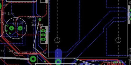
    I've had the same issue in the past. The only way I know is to just reduce the track thickness manually (see example image below), as you

    approach very close to the pad.

    Ideally, it would be good if EAGLE would automatically reduce the thickness, and have a way not to cause a DRC error (since typically, the

    thick tracks would have a class) as long as the track is only thin to within x mil (i.e. it should be configurable) distance of the pad.

    Note: this is with v5, perhaps v6 has an enhancement in this area.


    You can see a type of example here (which is a partially laid out board). In this case, the fat tracks were not for current

    capability but for controlled impedance, but I need to make them narrower as they approach close to the pads, otherwise they would not fit.

    image

    • Cancel
    • Vote Up 0 Vote Down
    • Sign in to reply
    • Cancel
  • autodeskguest
    autodeskguest over 13 years ago in reply to shabaz

    On 04/18/2013 06:33 AM, shabaz wrote:

    Hi Norm,


    I've had the same issue in the past. The only way I know is to just

    reduce the track thickness manually (see example image below), as you

    approach very close to the pad.

    I use polygons for power and ground traces. DRC takes care of clearances

    so you don't have to be exact.

    Paul R


    • Cancel
    • Vote Up 0 Vote Down
    • Sign in to reply
    • Cancel
  • shabaz
    shabaz over 13 years ago in reply to autodeskguest

    Hi Paul,


    Good point, that works well for a few major traces.

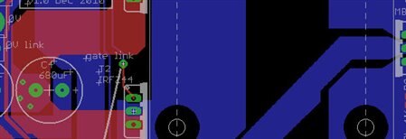
    @Norm, An example is below using the polygon method.


    If you want to reduce a track width, select the 'route manually' icon

    on the left side icons, and then click on a yellow wire, and then left-clicking to route it until you reach close to the pad,

    then go to the top and change width, and then finally click inside the pad to end the yellow wire.


    As drawn:

    image

    What it looks like:

    image

    • Cancel
    • Vote Up 0 Vote Down
    • Sign in to reply
    • Cancel
Reply
  • shabaz
    shabaz over 13 years ago in reply to autodeskguest

    Hi Paul,


    Good point, that works well for a few major traces.

    @Norm, An example is below using the polygon method.


    If you want to reduce a track width, select the 'route manually' icon

    on the left side icons, and then click on a yellow wire, and then left-clicking to route it until you reach close to the pad,

    then go to the top and change width, and then finally click inside the pad to end the yellow wire.


    As drawn:

    image

    What it looks like:

    image

    • Cancel
    • Vote Up 0 Vote Down
    • Sign in to reply
    • Cancel
Children
No Data
element14 Community

element14 is the first online community specifically for engineers. Connect with your peers and get expert answers to your questions.

  • Members
  • Learn
  • Technologies
  • Challenges & Projects
  • Products
  • Store
  • About Us
  • Feedback & Support
  • FAQs
  • Terms of Use
  • Privacy Policy
  • Legal and Copyright Notices
  • Sitemap
  • Cookies

An Avnet Company © 2026 Premier Farnell Limited. All Rights Reserved.

Premier Farnell Ltd, registered in England and Wales (no 00876412), registered office: Farnell House, Forge Lane, Leeds LS12 2NE.

Follow element14

  • X
  • Facebook
  • linkedin
  • YouTube