I reviewed the PDF that covers ULP.... User Language Programs ...... and I could not see a way to automate creating a layout.
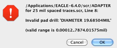
I want to create a layout without a schematic. I am creating a set of traces that are spaced 25 mils apart.
Each trace is terminated with a via that has a pad size diameter of 75 mils. In order to get the pads to fit I am staggering them in groups of four.
Anyway, it would be great if I could write an ULP that would lay down *n* traces spaced 25 mils apart. Each trace would be shorter until the fifth one which would start getting longer. Is it possible to write an ULP that creates a new layout, and then lays down the pads and traces ?
I can figure out the logic of the program... I jsut need the syntax ( if it exists ) for creating traces and vias.
This will result in an adapter pattern that I can use for chips with 25 mil lead spacing.....
Thanks
Gus S. Calabrese @99guspuppet
 |