element14 Community
element14 Community
    Register Log In
  • Site
  • Search
  • Log In Register
  • Community Hub
    Community Hub
    • What's New on element14
    • Feedback and Support
    • Benefits of Membership
    • Personal Blogs
    • Members Area
    • Achievement Levels
  • Learn
    Learn
    • Ask an Expert
    • eBooks
    • element14 presents
    • Learning Center
    • Tech Spotlight
    • STEM Academy
    • Webinars, Training and Events
    • Learning Groups
  • Technologies
    Technologies
    • 3D Printing
    • FPGA
    • Industrial Automation
    • Internet of Things
    • Power & Energy
    • Sensors
    • Technology Groups
  • Challenges & Projects
    Challenges & Projects
    • Design Challenges
    • element14 presents Projects
    • Project14
    • Arduino Projects
    • Raspberry Pi Projects
    • Project Groups
  • Products
    Products
    • Arduino
    • Avnet & Tria Boards Community
    • Dev Tools
    • Manufacturers
    • Multicomp Pro
    • Product Groups
    • Raspberry Pi
    • RoadTests & Reviews
  • About Us
  • Store
    Store
    • Visit Your Store
    • Choose another store...
      • Europe
      •  Austria (German)
      •  Belgium (Dutch, French)
      •  Bulgaria (Bulgarian)
      •  Czech Republic (Czech)
      •  Denmark (Danish)
      •  Estonia (Estonian)
      •  Finland (Finnish)
      •  France (French)
      •  Germany (German)
      •  Hungary (Hungarian)
      •  Ireland
      •  Israel
      •  Italy (Italian)
      •  Latvia (Latvian)
      •  
      •  Lithuania (Lithuanian)
      •  Netherlands (Dutch)
      •  Norway (Norwegian)
      •  Poland (Polish)
      •  Portugal (Portuguese)
      •  Romania (Romanian)
      •  Russia (Russian)
      •  Slovakia (Slovak)
      •  Slovenia (Slovenian)
      •  Spain (Spanish)
      •  Sweden (Swedish)
      •  Switzerland(German, French)
      •  Turkey (Turkish)
      •  United Kingdom
      • Asia Pacific
      •  Australia
      •  China
      •  Hong Kong
      •  India
      •  Korea (Korean)
      •  Malaysia
      •  New Zealand
      •  Philippines
      •  Singapore
      •  Taiwan
      •  Thailand (Thai)
      • Americas
      •  Brazil (Portuguese)
      •  Canada
      •  Mexico (Spanish)
      •  United States
      Can't find the country/region you're looking for? Visit our export site or find a local distributor.
  • Translate
  • Profile
  • Settings
Autodesk EAGLE
  • Products
  • More
Autodesk EAGLE
EAGLE User Support (English) Complex polygons on stopmask layer (tstop/bstop)
  • Blog
  • Forum
  • Documents
  • Events
  • Polls
  • Files
  • Members
  • Mentions
  • Sub-Groups
  • Tags
  • More
  • Cancel
  • New
Join Autodesk EAGLE to participate - click to join for free!
Actions
  • Share
  • More
  • Cancel
Forum Thread Details
  • State Verified Answer
  • Replies 2 replies
  • Subscribers 179 subscribers
  • Views 917 views
  • Users 0 members are here
  • tstop
  • polygon
  • soldermask
Related

Complex polygons on stopmask layer (tstop/bstop)

Former Member
Former Member over 10 years ago

Is there any way to specify a region (sub-polygon) within a tstop polygon where there should be soldermask?


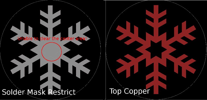
I'm designing a series of Christmas ornaments to give away as gifts. I've created a number of simple motifs (example... snowflake) within AutoCAD and then imported them as polygons into EAGLE. By using multiple layered polygons and specifying cutout fills on a few of them I can successfully create the desired images within the copper layer. The issue is that I was wanting to have this copper exposed for gold surface plating and I am unable to get the proper effect with the soldermask restrict layers. Currently I am only able to make polygons on the tstop layer that remove soldermask, I am unable to make any sort of "cutout" regions where there should be soldermask, for example in the center of a snowflake. I'm not willing to leave these regions exposed since there won't be any copper there and the bare FR4 will be showing. (ugly...)


Likewise I can't simply leave the entire top layer of the board a copper pour and put the image in the tstop layer since the same issue with internal areas will still be there. (I would only be able to do an external outline of the motif...) Not to mention I will be placing numerous 0402 LED's around on the ornament, and the clearance between the pads and pour would make them more visible. I've tried using a number of copy-layer-to-layer ULP's but none of them have been able to replicate the cutout effect.


I know how to properly do this in KiCAD and Altium, but would rather use EAGLE over KiCAD and it feels funny using work software for personal use. :-) Not to mention I've already made the schematic and libraries for this project and don't want to have to redo it all with the tight timeline I have.


Thanks for your suggestions!

-Brent


image

  • Sign in to reply
  • Cancel
  • autodeskguest
    0 autodeskguest over 10 years ago

    On 11/16/2015 02:06 PM, Brent Mellor wrote:

    Currently I am only able to make polygons on the tstop

    layer that remove soldermask, I am unable to make any sort of "cutout"

    regions where there should be soldermask

    Two ways.

    1. Use lines on tstop and bstop to cover the area.

    2. Duplicate the copper layers to an unused copper layer and add them

    the the cam output for tstop/bstop.

    Paul


    • Cancel
    • Vote Up 0 Vote Down
    • Sign in to reply
    • Reject Answer
    • Cancel
  • Former Member
    0 Former Member over 10 years ago in reply to autodeskguest

    I see, so it's really only possible via modifying the CAM processing. We'll that shouldn't be hard at all... I can't believe that I hadn't thought of that!

    I'll mark this question as answered, but if anyone knows of any other tricks I would be interested to hear.


    Thanks

    -Brent

    • Cancel
    • Vote Up 0 Vote Down
    • Sign in to reply
    • Verify Answer
    • Cancel
element14 Community

element14 is the first online community specifically for engineers. Connect with your peers and get expert answers to your questions.

  • Members
  • Learn
  • Technologies
  • Challenges & Projects
  • Products
  • Store
  • About Us
  • Feedback & Support
  • FAQs
  • Terms of Use
  • Privacy Policy
  • Legal and Copyright Notices
  • Sitemap
  • Cookies

An Avnet Company © 2025 Premier Farnell Limited. All Rights Reserved.

Premier Farnell Ltd, registered in England and Wales (no 00876412), registered office: Farnell House, Forge Lane, Leeds LS12 2NE.

ICP 备案号 10220084.

Follow element14

  • X
  • Facebook
  • linkedin
  • YouTube