


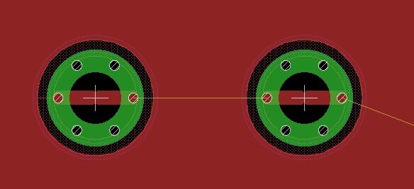
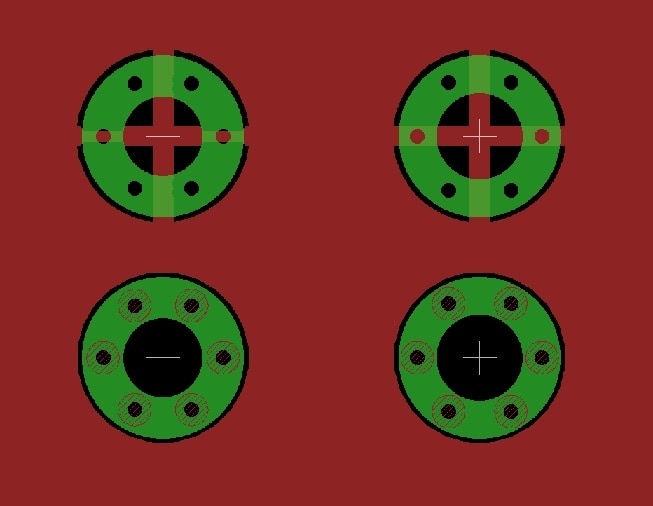
I'm looking for a way to create mounting hole with 6 vias (as a library component) for M3 screw. I was able to create such a package but when I use it on a board and run DRC, I get "Overlap" errors. The vias are defined as small pads since vias are not available in library designer. Is there a way to get rid of the errors? I remember that I was able to define such a component in KiCAD and I' surprised that in Eagle it is that difficult.
Here: pcb design - Mounting hole on a PCB - Electrical Engineering Stack Exchange is an example of such a mounting hole (the right most on the photo).
Mark

